Global high-mix volume high-speed PCBA manufacturer
9:00 -18:00, Mon. - Fri. (GMT+8)
9:00 -12:00, Sat. (GMT+8)
(Except Chinese public holidays)
Global high-mix volume high-speed PCBA manufacturer
9:00 -18:00, Mon. - Fri. (GMT+8)
9:00 -12:00, Sat. (GMT+8)
(Except Chinese public holidays)
HomePage > Blog > Knowledge Base > PCB Copper Plating — Process, Types, Standards, and Best Practices
In electronics manufacturing, PCB copper plating is a key process to ensure the high reliability of circuit boards. Whether it is smartphones, wearable devices, automotive systems or industrial equipment, they all rely on copper PCB circuit boards to achieve electrical connections, mechanical stability and thermal management. It is the PCB plating process that establishes the conductive network required by these devices, enabling the circuit boards to operate stably in various environments.
The electroless plating of copper and electrolytic copper plating on PCBs together form a complete process. Each is responsible for different stages to ensure the production of high-performance and reliable copper circuit boards. These processes require precise design, professional chemical treatment, and compliance with industry standards in order to meet the modern circuit board's requirements for high density and high speed.
This article will introduce the PCB copper plating process, including plating types, process steps, industry standards, common defects and best practices. Whether it is a simple single-layer board or a complex HDI board, understanding PCB copper plating is the foundation for manufacturing high-quality circuit boards.

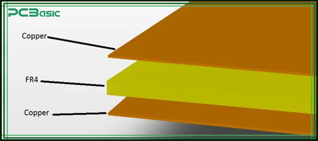
PCB copper plating refers to the process of depositing a layer of copper onto the copper layer on the surface of the PCB substrate to form conductive traces, pads and interconnections. This copper plating process enables copper PCB boards to transmit electrical signals, supply power, and provide mechanical support for components. Without reliable PCB copper plating, the circuit board will not function properly.
PCB copper plating mainly includes two methods:
Electroless Copper Plating
Electroless copper plating does not require an external current. The circuit board is immersed in a chemical solution, and through a chemical reduction reaction, a uniform thin copper layer is formed on the surface and hole walls. This step is mainly used to establish an initial conductive layer on the non-conductive surface to provide a foundation for subsequent electrolytic plating. The thickness of the copper layer in electroless plating of copper is typically 0.1–0.5 microns.
Electrolytic Copper Plating
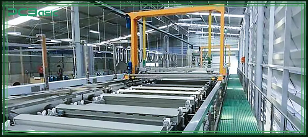
Electrolytic copper plating requires an electric current. The circuit board is placed in an electrolyte solution (such as copper sulfate solution), and under the action of the current, copper ions are deposited onto the traces, pads, and hole walls to increase the copper layer thickness and improve conductivity and mechanical strength. Electrolytic PCB copper plating is used to form the final copper thickness according to design requirements; for example, 1 oz copper thickness equals 35 microns.
The combination of these two types forms a complete PCB plating process, creating strong and reliable conductive paths for the copper PCB board.
When manufacturing copper PCB boards, PCB copper plating is very important. This process is directly related to the performance and reliability of the circuit board. The reasons mainly include the following points.
Electrical Conductivity:
Copper plating can form a continuous conductive layer on the circuit board. This copper layer has low resistance and can achieve high-speed signal transmission and stable power distribution. A good PCB copper conductive layer can ensure that the copper PCB board operates normally as per the design requirements under various working conditions.
Mechanical Strength:
In the PCB copper plating process, the electroplated copper layer covers the through-hole walls and strengthens the connections between the layers. This enables the copper PCB board to maintain a stable structure when subjected to external shocks, vibrations or temperature changes, and is not prone to breakage or damage.
Thermal Management:
The plated copper layer in PCB copper can quickly conduct heat generated by components. Effective copper plating can prevent performance degradation or component failure of the circuit board caused by overheating. This is particularly important for high-power circuit boards.
Corrosion Resistance:
High-quality PCB copper plating can form a protective layer on the surface of copper PCB boards. This protective layer can prevent oxygen or moisture in the air from reacting with the copper, avoiding oxidation and corrosion, thereby extending the service life of the circuit board and enhancing overall reliability.
By precisely controlling each step of the PCB plating process, manufacturers can produce copper PCB boards that can still operate stably in harsh environments such as high temperature, high humidity or high vibration.

The PCB plating process used for manufacturing high-reliability copper PCB boards consists of multiple key steps. Each step needs to be precisely controlled to ensure a uniform copper layer and strong adhesion and to avoid common defects.
Drilling is the first step in the PCB plating process. This step involves drilling vias and through holes at the positions required for PCB copper plating through high-precision mechanical drilling. These holes are used for subsequent electrical connections and interconnections between layers. The drilling accuracy directly affects the deposition quality of the later copper layer.
Deburring is used to remove burrs and debris produced during the drilling process, making the hole walls smooth and flat. Cleaning is used to thoroughly remove oil stains, dust and drill chips from the surface and holes of PCB boards. Good deburring and cleaning processes are the prerequisites for ensuring the success of the subsequent copper plating process. If not cleaned thoroughly, the copper layer may not adhere firmly.
Activation involves chemically treating the hole walls to provide catalytic activity on the surface. This step provides the necessary conditions for electroless PCB plating. The activator is evenly attached to the hole wall and the plate surface, enabling the subsequent electroless copper plating to form a continuous copper layer on non-conductive materials.
Electroless copper plating does not require an external current. During the chemical reaction, copper ions are uniformly deposited throughout the surface and hole walls, forming an initial thin copper layer. This layer of copper provides a seed layer for electrolytic copper plating, and its thickness is generally within the range of 0.1 to 0.5 microns.
Pattern imaging is used to define the areas that require additional copper plating. The photoresist is coated on the board surface through the photolithography process, and the circuit pattern area is exposed and developed. This step determines the specific traces of the circuit and the position of the solder pads.
Electrolytic copper plating is an important step in selectively increasing the thickness of the copper layer in the defined area. In the electrolyte solution with applied current, copper ions are deposited on the traces, pads and through-hole walls of the PCB board. This step ensures that the copper layer thickness meets the design requirements. For example, the thickness of 1 oz copper is approximately 35 micrometers. Electrolytic copper electroplating can enhance its electrical conductivity and mechanical strength.
Etching is used to remove the unprotected excess copper layer. The chemical etchant removes the unwanted copper, leaving only the precise traces and pad patterns formed by PCB copper plating. This step determines the accuracy and integrity of the final circuit.
Surface finish is the final step of the PCB copper plating process. Common surface finishes include ENIG (electroless nickel gold), OSP (organic solderability preservative), and HASL (hot air solder leveling). These finishes can prevent the oxidation of the PCB copper layer and ensure good solderability, enhancing the long-term reliability of the circuit board.
Each step of the PCB plating process requires strict process control. Only in this way can defects be prevented, the uniform distribution of the copper layer be ensured, and copper PCB boards of high quality and high reliability be produced.
 About PCBasic
Time is money in your projects – and PCBasic gets it. PCBasic is a PCB assembly company that delivers fast, flawless results every time. Our comprehensive PCB assembly services include expert engineering support at every step, ensuring top quality in every board. As a leading PCB assembly manufacturer, we provide a one-stop solution that streamlines your supply chain. Partner with our advanced PCB prototype factory for quick turnarounds and superior results you can trust.
PCB copper plating needs to comply with strict industry standards to ensure that the electrical performance, mechanical strength and thermal performance of the circuit board meet the requirements and satisfy the demands of high-reliability applications.
Common copper plating standards include:
• IPC-6012 / IPC-6012B and later versions
These standards specify the required copper thickness for the external and internal layers of rigid copper PCB boards. For via-in-pad structures, the standards require copper wrap plating to ensure that the copper layer extends continuously from the hole wall to the surface pad, thereby enhancing interconnection strength and soldering reliability.
• IPC-2221
This standard provides design guidelines for trace width and spacing to ensure that the circuit pattern aligns with the capabilities of the PCB plating process and meets electrical performance requirements.
Adhering to the above copper plating standards can ensure that PCB copper boards have excellent electrical interconnection performance, mechanical stability and solderability in highly reliable applications and can adapt to harsh working environments such as high temperature, high humidity and high vibration.
In the PCB copper plating process, even with mature processes and equipment, some common defects may still occur. If these defects are not detected and resolved in time, they can affect the electrical performance and reliability of the copper PCB board.
Pitting
Pitting refers to the appearance of tiny holes or rough spots on the surface of the copper layer. This defect is usually caused by impurities or particles in the copper plating solution. During the plating process, impurities adhere to the surface, leading to uneven copper deposition.
Nodules / Protrusions
Nodules or protrusions refer to excessive copper buildup in local areas, forming bumps or lumps. This is usually caused by uneven current distribution or improper control of plating parameters, which can result in uneven trace or pad surfaces.
Poor Adhesion
If the cleaning or surface preparation in the earlier stages is insufficient, the adhesion between the copper layer and the substrate will be weak. This can cause the copper layer to peel off or crack during subsequent processes or use, seriously affecting the reliability of the PCB copper plating.
Uneven Plating
Uneven plating is manifested as significant differences in copper thickness across different areas. This is mostly caused by uneven current distribution or inconsistent process parameter control, which can lead to unstable electrical performance.
Contamination
If rinsing is not thorough, residual chemicals may contaminate subsequent plating bath solutions or surfaces, affecting the quality and appearance of the copper layer. Contamination can also cause soldering difficulties or reduce long-term reliability.
To reduce defects in the PCB copper plating process, the following measures are recommended:
Keep process bath solutions and rinse water clean. Regularly filter and replace chemical solutions to prevent the accumulation of impurities. Use sufficient clean water during rinsing to avoid residual contaminants.
Precisely control chemical concentrations and plating parameters. Strictly monitor current density, temperature, solution composition, and stirring speed to ensure uniform and consistent copper plating.
Regularly inspect the copper PCB board and perform cross-section analysis. Use microscopy to observe copper layer thickness and hole wall coverage to detect and correct potential issues in a timely manner.
The success of any copper PCB board depends on the precision and quality of its PCB copper plating. Whether it is the electroless plating of copper on a PCB or the plating of electrolytic copper, both are crucial for creating conductive paths, mechanical stability and reliable heat dissipation.
Through strict process control, compliance with industry standards and application of best practices, manufacturers can ensure the production of robust and high-performance copper circuit boards. With the development of technology, innovative PCB plating methods such as direct metallization and pulse plating will continue to enhance the quality and sustainability of PCB copper plate manufacturing.
Whether it is designing a simple single-layer board or a complex HDI structure, understanding the PCB copper plating process is the key to achieving outstanding results in modern electronic manufacturing.

Assembly Enquiry
Instant Quote
Phone contact

+86-755-27218592
In addition, we've prepared a Help Center. We recommend checking it before reaching out, as your question and its answer may already be clearly explained there.
Wechat Support

In addition, we've prepared a Help Center. We recommend checking it before reaching out, as your question and its answer may already be clearly explained there.
WhatsApp Support

In addition, we've prepared a Help Center. We recommend checking it before reaching out, as your question and its answer may already be clearly explained there.