Global high-mix volume high-speed PCBA manufacturer
9:00 -18:00, Mon. - Fri. (GMT+8)
9:00 -12:00, Sat. (GMT+8)
(Except Chinese public holidays)
Global high-mix volume high-speed PCBA manufacturer
9:00 -18:00, Mon. - Fri. (GMT+8)
9:00 -12:00, Sat. (GMT+8)
(Except Chinese public holidays)
HomePage > Blog > Knowledge Base > PCB Types: A Comprehensive Guide
It can be said that the printed circuit board is the core of all modern electronic boards. PCB plays a crucial role in smartphones, smart home devices, industrial sensors, automotive control units and medical equipment. With the continuous development of electronic products towards miniaturization, high density and high speed, the types and manufacturing processes of circuit boards have also diversified accordingly. Different application scenarios require the selection of different PCB types.
Understanding different types of PCBs, their structural characteristics, material advantages and applicable scenarios is the basis for enhancing product competitiveness and ensuring high-quality production. In this article, we will comprehensively analyze various types of PCB boards and their applications. This article can help you make more scientific and efficient decisions in selection and design. Next, let's directly enter the topic of the article - PCB types!
Each type of circuit board varies in structure, number of layers, materials and manufacturing processes. When choosing the appropriate PCB type, factors such as component density, signal transmission speed, power consumption requirements and usage environment also need to be considered. Next, we will delve into the common types of PCBs, introducing their structural characteristics, commonly used materials, advantages and limitations.
Single-sided PCB (also known as single-layer PCB) is the most fundamental type among all PCB board types. This kind of circuit board is composed of a conductive copper layer and an insulating substrate. All the electronic components on it are installed on the same side, and the electrical connection between the components is achieved by copper traces.
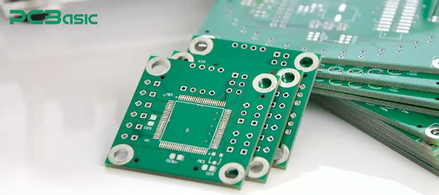
The typical structures of single-layer PCBs include:
Substrate layer: FR4, CM-1 or aluminum-based materials are usually used to provide mechanical strength.
Single-layer copper foil: forms circuit patterns to achieve electrical connections.
Solder mask layer: covered with copper foil to prevent oxidation and short circuits.
Silk-screen layer: used for component identification and installation positioning.
Since a single-layer PCB has only one layer of copper foil, the wiring must be carefully planned to avoid crossing the traces. Compared with multi-layer PCB types, single-layer boards have more limitations in circuit design.
Common materials for single-layer PCBs include:
FR4: This is the most common material and is suitable for low-cost, standard applications.
CEM-1: It is a low-cost alternative to FR4 and is often used in non-critical simple circuits.
Metal core PCB: Suitable for applications that require heat dissipation. For instance, LED circuit boards often combine copper layers with aluminum bases to enhance thermal conductivity.
Tips: Even for the simplest single-layer PCB board, material selection is of crucial importance.
Single-layer PCBs have a simple structure, use fewer materials, and have a relatively low manufacturing cost. The simple design enables it to have a fast production cycle, making it highly suitable for mass production of low-complexity electronic boards. However, single-layer PCBs have significant limitations in complex circuits or high-performance applications. Compared with high-end circuit board types such as multi-layer PCBs or HDI PCBs, single-layer PCBs are difficult to meet the design requirements of modern miniaturized and high-performance electronic devices.
Most single-layer PCBs will adopt basic PCB surface finish types, such as hot air leveling (HASL), to reduce costs. The soldering process of single-layer PCBs is usually also relatively simple. Reflow soldering is mostly adopted in mass production. Of course, different types of PCB solders are also chosen based on the type of components.
Single-layer PCBs are an ideal choice for cost-sensitive electronic applications with low complexity requirements. Although its functions are limited, single-layer boards still play an irreplaceable role in many low-complexity devices.
Double-layer boards have copper foil on both sides of the insulating substrate. It connects the circuits on both sides through through holes. Compared with single-layer PCBs, double-layer circuit boards offer greater wiring flexibility. It is widely used in medium-complexity equipment such as power supplies and instruments.
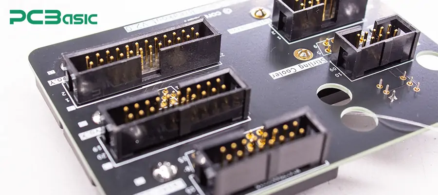
Both copper layers of a double-layer PCB can be wired, and they are electrically connected through through holes. It supports higher density and more complex circuit designs. The commonly used materials are:
FR4: The most common, suitable for general electronic products.
CEM-3: Similar to FR4, but with a lower cost.
The typical structures of double-sided PCBs include:
Upper and lower copper layers: Located on both sides of the PCB respectively, they are used for wiring and soldering components.
Insulating substrate: Materials such as FR4 and CEM-3 are usually selected to provide mechanical strength and insulation performance for circuit boards.
Through hole: Electrical intercommunication is achieved by connecting the upper and lower copper foils through a metalized hole.
Solder mask layer: It covers a copper layer to prevent oxidation, short circuit and protect the wiring.
Silk-screen layer: It is used to mark the position, number and other information of components.
The routing capability of double-layer PCBs is enhanced, enabling them to support more complex designs than single-layer boards. And the cost is moderate and the technology is mature. However, it is not suitable for applications with extremely high-density or high-speed signals. Common surface treatments include HASL, OSP and gold plating. The commonly used soldering types are wave soldering, manual soldering and reflow soldering.
A multi-layer PCB is a circuit board composed of 4, 6, 8 or more copper layers stacked together. This type of circuit board is suitable for high-density and complex circuits, such as those in smartphones, computers, and industrial control devices. It achieves interlayer interconnection through inner layers and blind/buried vias and is the core of modern high-density electronic devices.
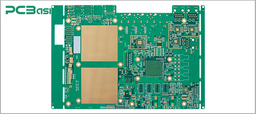
Multi-layer PCBs typically consist of the following components:
Inner circuit layer: It is used for signal transmission, power distribution and ground layer, and supports high-frequency and high-speed signal integrity design.
Dielectric layer: Located between the conductive layers, it is used for electrical isolation and provides mechanical strength.
Outer circuit layer: Used for soldering components and connecting external interfaces.
Blind holes/buried holes/through holes: Used for interconnection between different layers to achieve a compact routing solution.
Multi-layer PCBs support more complex circuit layouts. It can separate the signal layer, power layer and ground layer, thereby optimizing electromagnetic compatibility (EMC) performance and signal integrity.
The commonly used materials for multi-layer circuit boards are high-quality FR4 or special high-speed materials (such as Rogers, PTFE), which are often used in high-speed and high-frequency applications. This type of PCB has the capability of high-density wiring. It supports high-speed and high-frequency circuits. However, its manufacturing cost is high, its process is complex, and its maintenance is also difficult.
Rigid PCBs are made of hard materials such as FR4, and this type of PCB provides good mechanical support for components. It is commonly used in consumer electronics and automotive electronics. Rigid PCBs cannot be bent and their shapes are fixed. It can be single-layer, double-layer or multi-layer.
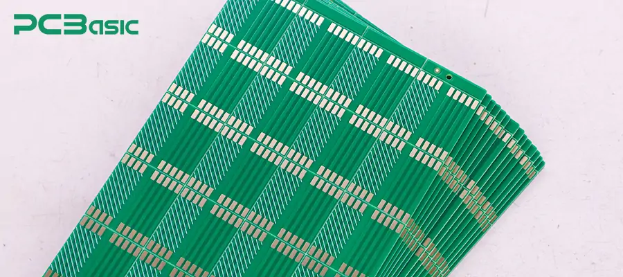
Common materials
FR4, CEM series.
High TG materials are used in high-temperature resistant environments.
Advantages of rigid PCBs
It has high mechanical strength and is easy to fix and assemble.
Disadvantages of rigid PCBs
It is not suitable for equipment that requires dynamic bending.
Surface treatment and soldering of rigid PCBs
Common surface treatment methods include HASL and gold plating.
Common soldering methods include wave soldering, reflow soldering, etc.
Flexible PCBs are made of materials such as polyimide. This kind of PCB can be bent and folded inside the device and is suitable for wearable devices, medical devices and cameras. It features ultra-thinness and lightweight, making it highly suitable for the demands of miniaturized electronic devices. Meanwhile, it can adapt to dynamic bending scenarios and meet the requirements of special applications such as wearables and medical care. The commonly used materials for it are polyimide and polyester.
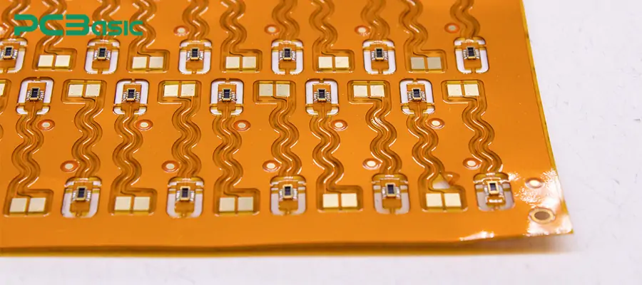
Advantages of flexible PCBs
Saves space and is suitable for miniaturization.
Good dynamic performance.
Disadvantages of flexible PCBs
High cost, high soldering requirements.
Surface treatment and soldering of flexible PCBs
Commonly used ones include gold plating, tin plating, OSP, etc.
Soldering mainly adopts reflow soldering and manual soldering.
Rigid-flex PCB is a combination of rigid and flexible circuit boards. It has obvious advantages in complex and compact designs and is suitable for complex three-dimensional structure designs.
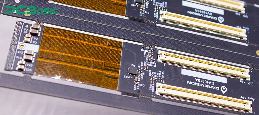
Rigid-flex boards combine the advantages of both rigid and flexible circuit boards. The rigid zone is used to support electronic components, providing excellent mechanical strength and stability. The flexible area is used to achieve the bending connection, enabling the circuit to adapt to the three-dimensional spatial layout. This structure enables the rigid-flexible composite board to perform well in applications with high density and high reliability requirements.
Rigid-flexible composite panels typically use FR4 as the rigid layer to provide strength and support. The flexible layer mostly selects polyimide material, which has excellent heat resistance and bendability.
Advantages of rigid-flex PCBs
Compact structure and high reliability.
Optimize the assembly process.
Disadvantages of rigid-flex PCBs
The manufacturing cost is high and the design requirements are high.
Surface treatment and soldering of rigid-flex PCBs
The main methods adopted are gold plating and OSP.
Soldering is mostly reflow soldering + local manual soldering.
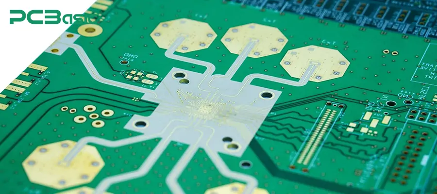
High-frequency PCBs are mainly designed to handle radio frequency or microwave signals. Therefore, the routing requirements for high-frequency PCBs are precise, and the routing design needs to strictly control the impedance. Only in this way can signal integrity and low-loss transmission be ensured.
Common materials for high-frequency PCBs include PTFE (Teflon), Rogers boards and ceramic substrates. These materials have low dielectric constant and low dielectric loss, which can effectively reduce the attenuation of high-frequency signals. Moreover, these materials possess excellent high-frequency electrical properties and stable dielectric characteristics, making them suitable for demanding high-frequency and high-speed circuit design requirements.
Advantages of high-frequency PCBs
Excellent high-frequency performance.
Disadvantages of high-frequency PCBs
The manufacturing process is complex and the cost is high.
Surface treatment and soldering of high-frequency PCBs
Common surface treatments include gold plating, silver plating, nickel-gold plating, etc.
Soldering mainly involves high-precision reflow soldering and selective soldering.
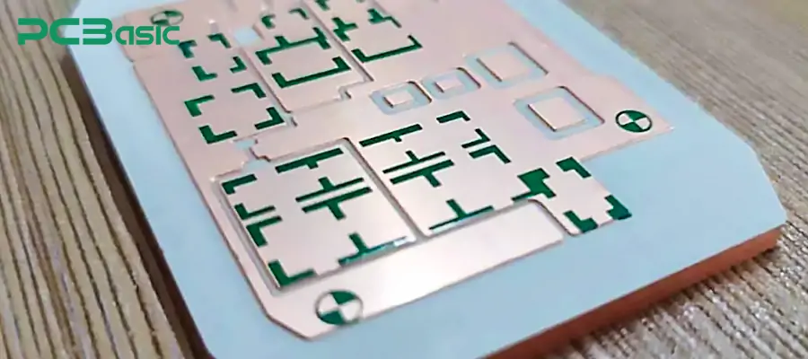
The aluminum-backed PCB has excellent heat dissipation performance. This performance makes it highly suitable for fields with high heat dissipation requirements such as LED lighting and power electronics. Aluminum-backed PCBs are typically composed of copper layers, insulating layers and aluminum substrates. These three layers of structure are closely combined to meet the heat dissipation requirements of high-power electronics.
This type of circuit board has a high thermal conductivity and excellent heat dissipation performance. It can effectively reduce the operating temperature of electronic components and extend the service life of the products. The base material of aluminum-backed PCBs mainly adopts high-purity aluminum substrates. Copper substrates are also used in some high-end applications to meet higher requirements for thermal conductivity and mechanical strength.
Advantages of aluminum-backed PCB
Excellent heat dissipation capacity.
Disadvantages of aluminum-backed PCB
Not suitable for high-frequency and high-density design.
Surface treatment and soldering of aluminum-backed PCB
Surface treatment: HASL, OSP.
Soldering: wave soldering, manual soldering or dedicated high-power soldering.
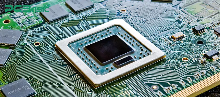
HDI PCB is a type of circuit board that adopts small through vias, fine wire widths and high-density wiring. It is applicable to modern highly integrated electronic products. It supports smaller component packages, such as BGA, CSP, etc., which helps to achieve miniaturization and high-performance design.
Meanwhile, HDI PCB optimizes impedance control and is highly suitable for high-speed signal transmission and high-frequency applications. High-performance FR4 is commonly used as the base material for HDI PCBs to balance cost and performance. In higher-demand high-speed and high-frequency designs, high-speed and low-loss materials such as Rogers boards and Panasonic Megtron series will also be selected. This can better ensure excellent electrical performance and stability.
Advantages of HDI PCBs
Achieve smaller size and higher functional density.
Support high-speed signals and precision components.
Disadvantages of HDI PCBs
The manufacturing process is complex and the cost is relatively high.
The design and production cycle is longer.
Surface treatment and soldering of HDI PCBs
Commonly used high-end surface treatments include gold plating (ENIG), silver plating, and chemical nickel palladium gold plating.
The main soldering processes are reflow soldering and selective soldering.
|
PCB Type |
Main Structural Features |
Advantages |
Disadvantages |
Typical Applications |
|
Single-layer PCB |
Single copper layer + insulating substrate |
Low cost, simple design, ideal for mass production |
Limited circuit complexity, not suitable for high-frequency or high-density designs |
Simple electronics, LED boards, remote controls |
|
Double-layer PCB |
Copper layers on both sides, connected by through-holes |
More flexible routing, supports medium complexity circuits |
Not suitable for ultra-high-density or high-speed signal applications |
Power supplies, appliances, instrumentation |
|
Multi-layer PCB |
Multiple copper layers stacked with insulating layers, blind/buried vias |
High-density routing, supports high-speed and high-frequency |
High manufacturing cost, complex process, difficult to repair |
Smartphones, computers, industrial controls |
|
Rigid PCB |
Rigid FR4 or CEM base material |
High mechanical strength, easy to mount and assemble |
Not suitable for dynamic bending |
Consumer electronics, automotive electronics |
|
Flexible PCB |
Flexible polyimide or polyester substrate |
Space-saving, ideal for miniaturization, good dynamic performance |
High cost, high soldering requirements |
Medical devices, wearables, camera modules |
|
Rigid-Flex PCB |
Combination of rigid and flexible areas |
Compact structure, high reliability, optimized assembly process |
High manufacturing cost, complex design |
Aerospace, military, high-end portable devices |
|
High-frequency PCB |
Low dielectric loss material, fine traces, strict impedance control |
Excellent high-frequency performance, good signal integrity |
Complex manufacturing, high cost |
RF modules, telecom equipment, radar |
|
Aluminum-backed PCB |
Copper layer + insulating layer + aluminum base |
Excellent heat dissipation, high thermal conductivity |
Not suitable for high-frequency or high-density circuits |
LED lighting, power electronics |
|
HDI PCB |
Microvias, fine lines, high-density interconnect |
Miniaturization, high integration, supports high-speed signals |
Complex process, high cost, longer production cycle |
Smartphones, tablets, high-speed data devices |
In addition to these common PCB types, there are also some special circuit board types designed for specific applications. For instance, ceramic PCBs, transparent PCBs, etc. Ceramic PCBs have excellent thermal conductivity and stability. It is widely applied in high-power modules, radio frequency and microwave circuits. Transparent PCBs are made of transparent substrates and have good light transmittance. It can not only achieve electrical connection but also meet the requirements of optical design.
Choosing the appropriate PCB type is the key to ensuring a good balance among performance, cost and reliability of electronic boards. By understanding different types of PCBs, materials, connectors, coatings and soldering types, we can design the best solutions for modern electronic products. Whether you need a simple single-layer board or a complex HDI board, working with a professional PCB manufacturer is the guarantee for achieving high-quality products.
 About PCBasic
Time is money in your projects – and PCBasic gets it. PCBasic is a PCB assembly company that delivers fast, flawless results every time. Our comprehensive PCB assembly services include expert engineering support at every step, ensuring top quality in every board. As a leading PCB assembly manufacturer, we provide a one-stop solution that streamlines your supply chain. Partner with our advanced PCB prototype factory for quick turnarounds and superior results you can trust.
Assembly Enquiry
Instant Quote
Phone contact

+86-755-27218592
In addition, we've prepared a Help Center. We recommend checking it before reaching out, as your question and its answer may already be clearly explained there.
Wechat Support

In addition, we've prepared a Help Center. We recommend checking it before reaching out, as your question and its answer may already be clearly explained there.
WhatsApp Support

In addition, we've prepared a Help Center. We recommend checking it before reaching out, as your question and its answer may already be clearly explained there.