Global high-mix volume high-speed PCBA manufacturer
9:00 -18:00, Mon. - Fri. (GMT+8)
9:00 -12:00, Sat. (GMT+8)
(Except Chinese public holidays)
Global high-mix volume high-speed PCBA manufacturer
9:00 -18:00, Mon. - Fri. (GMT+8)
9:00 -12:00, Sat. (GMT+8)
(Except Chinese public holidays)
HomePage > Blog > Knowledge Base > How to begin PCB Design and Assembly
In the world of electronics, Printed Circuit Boards (PCBs) play a crucial role in connecting and supporting electronic components. Whether you are designing a new gadget, an industrial device, or even a hobbyist project, understanding PCB design and assembly is fundamental.
This comprehensive guide will walk you through the key concepts of PCB design, what circuit boards are made of, how to design a PCB, and the steps involved in PCB assembly. Additionally, we’ll share valuable tips to help streamline the process, ensuring that your PCB projects are successful.

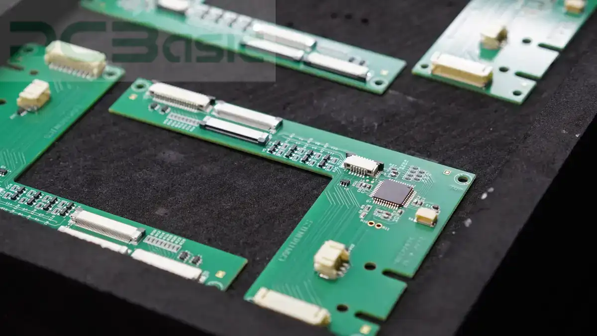
A Printed Circuit Board (PCB) is a flat, rigid board that serves as the foundation for connecting and supporting electronic components in an electronic device. It provides electrical connections via conductive tracks, pads, and other features etched into the board. Essentially, PCBs are the backbone of modern electronics, ensuring that signals and power flow correctly to different components.
PCBs are found in a wide range of devices, from smartphones and computers to household appliances and medical equipment. Without PCBs, the electronics we use today would not function as efficiently or compactly. The process of designing and assembling a PCB requires careful planning, precision, and an understanding of electrical engineering principles.
Circuit boards are typically made of multiple layers of materials that ensure both electrical conductivity and structural integrity. The primary materials used in PCB construction include:
Substrate (Base Material): The substrate is the foundation of the PCB and is often made from fiberglass (FR4) or other composite materials. This layer provides mechanical support and insulating properties.
Copper Layer: The copper layer is where electrical traces are etched to create conductive pathways. This layer is critical for connecting the electronic components on the PCB.
Solder mask: A thin layer of protective coating applied on top of the copper traces to prevent short circuits and ensure durability. It also helps identify the traces during assembly.
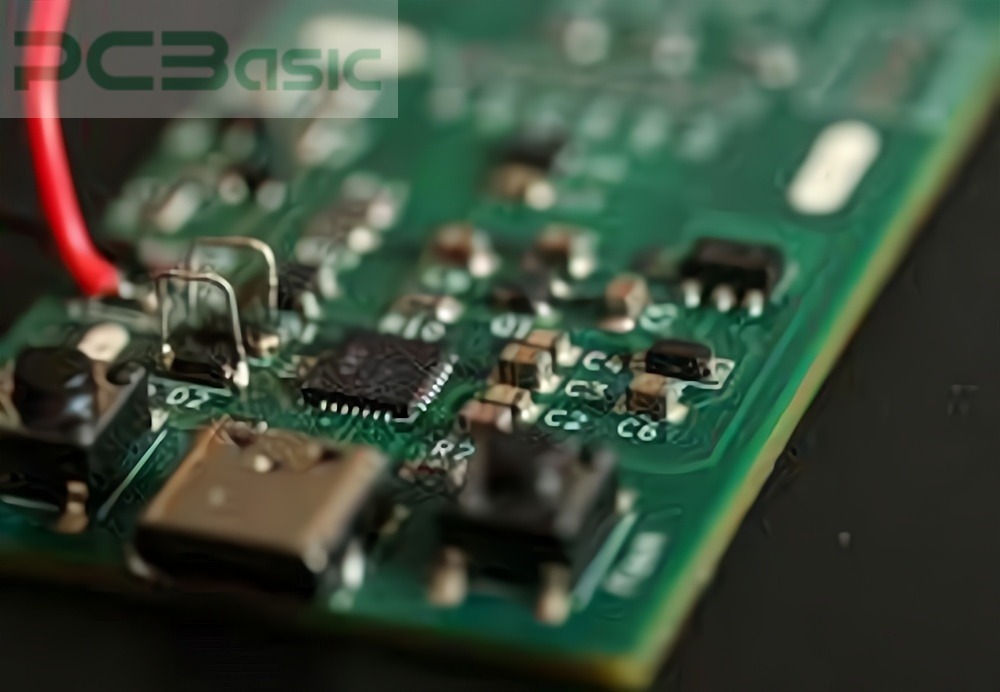
Silkscreen: This layer consists of text, symbols, and other markings that help identify components, pins, and connection points on the PCB.
In multilayer PCBs, there can be multiple layers of copper and insulating material, which increases the complexity but also allows for more compact designs.

Designing a PCB requires both creativity and technical skill. A well-designed PCB ensures reliable performance, manufacturability, and ease of assembly. Here are the basic steps involved in the PCB design process:
Before diving into the design process, it's essential to clearly define the functionality and specifications of your PCB. Determine the type of circuit (analog or digital), the power requirements, the size constraints, and any other specific needs, such as thermal management or electromagnetic interference (EMI) considerations.
A schematic is a visual representation of your electronic circuit, showing how components are connected. Tools like Eagle, KiCad, and Altium Designer can help create the schematic. It’s essential to choose the right components for your design and ensure they are properly rated for voltage, current, and other factors.
Once the schematic is complete, the next step is to lay out the PCB. This involves placing the components on the board and routing the electrical connections (traces). Key considerations during this phase include component placement for optimal signal integrity, minimizing cross-talk, and reducing the overall PCB size.
Once the layout is complete, it’s crucial to perform a Design Rule Check (DRC) to ensure that the design adheres to the manufacturing constraints. This includes verifying trace width, clearance between traces, and other critical parameters that affect the board’s functionality and manufacturability.
After verifying the design, the next step is to generate Gerber files, which are the standard file format used by PCB manufacturers. These files include all the information needed to produce the board, such as the copper layers, soldermask, and silkscreen.

PCB Assembly (PCBA) is the process of soldering components onto a PCB to create a fully functional circuit. It involves placing components such as resistors, capacitors, integrated circuits (ICs), and connectors onto the PCB, followed by soldering to form permanent electrical connections.
The assembly process can be done manually or automatically, depending on the scale and complexity of the project. Automated assembly techniques, such as Surface Mount Technology (SMT) or Through-Hole Technology (THT), are often used for mass production, while manual soldering may be employed for small runs or prototyping.
Assembling a PCB involves several steps, including component placement, soldering, and testing. Here’s a step-by-step overview of the PCB assembly process:
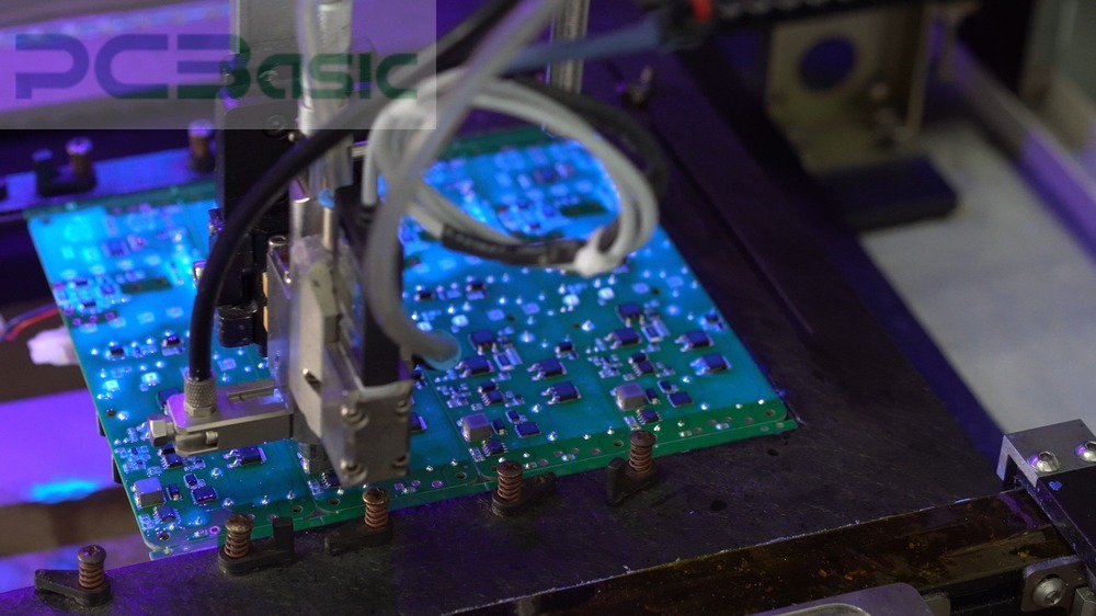
Ensure all components are available and properly organized. For surface-mount components, a pick-and-place machine is often used to place components on the board. For through-hole components, manual insertion or automated machines can be used.
Soldering is the process of using heat to melt solder onto the PCB, creating permanent electrical connections between the components and the traces. There are two main soldering techniques:
Wave Soldering: Used for through-hole components, where the PCB is passed over a wave of molten solder.
Reflow Soldering: Common for surface-mount components, where solder paste is applied, and the board is heated in an oven to melt the solder.
After soldering, the PCB is inspected for quality and reliability. Automated Optical Inspection (AOI) and X-ray inspection are often used for mass production to check for issues such as cold solder joints or misaligned components.
Finally, the assembled PCB undergoes electrical testing to ensure it functions correctly. This can include functional testing, where the board is tested in a real-world circuit, and in-circuit testing (ICT), which checks for shorts, open circuits, and other issues.

Plan for Manufacturability: During the PCB design phase, ensure that your design can be easily and cost-effectively manufactured. Avoid overly complex designs, and follow standard design rules to minimize production delays.
Consider the Design for Assembly (DFA): Choose components that are readily available, have a consistent footprint, and are easy to solder. Simplicity in the assembly process can reduce costs and increase the reliability of the final product.
Thermal Management: Ensure proper heat dissipation by placing heat-sensitive components away from heat sources and adding thermal vias or heat sinks as necessary.
Signal Integrity: Pay attention to trace widths, impedance control, and proper grounding to prevent issues such as noise and signal degradation, especially for high-frequency circuits.
Double-Check the Bill of Materials (BOM): Make sure that your BOM is complete, accurate, and up-to-date to avoid delays in the assembly process.
The process of PCB design and assembly is a detailed and technical journey, but with the right approach, it is manageable and rewarding. From understanding what a PCB is, to learning how circuit boards are made, and knowing the steps involved in designing and assembling a PCB, this guide has provided you with the essential knowledge. Whether you're a beginner or an experienced engineer, understanding the basics of PCB design, the materials used, and the steps to take from design to assembly will help you create high-quality, reliable electronic products. With the right tools, techniques, and attention to detail, your PCB projects will be well on their way to success.

Assembly Enquiry
Instant Quote
Phone contact

+86-755-27218592
In addition, we've prepared a Help Center. We recommend checking it before reaching out, as your question and its answer may already be clearly explained there.
Wechat Support

In addition, we've prepared a Help Center. We recommend checking it before reaching out, as your question and its answer may already be clearly explained there.
WhatsApp Support

In addition, we've prepared a Help Center. We recommend checking it before reaching out, as your question and its answer may already be clearly explained there.