Global high-mix volume high-speed PCBA manufacturer
9:00 -18:00, Mon. - Fri. (GMT+8)
9:00 -12:00, Sat. (GMT+8)
(Except Chinese public holidays)
Global high-mix volume high-speed PCBA manufacturer
9:00 -18:00, Mon. - Fri. (GMT+8)
9:00 -12:00, Sat. (GMT+8)
(Except Chinese public holidays)
HomePage > Blog > Knowledge Base > How Are Circuit Boards Made?
Printed circuit boards (PCBs) are the backbones of modern electronic equipment. No matter it is a small mobile phone, computer or other electronic equipment, or a variety of large complex industrial machines, circuit boards play an important role in ensuring their operation normal.
Although a PCB looks like a small and thin board, it actually contains a variety of complex circuits and connections that support the proper functioning of electronic devices. Understanding how circuit boards are made is key to appreciating their significance in modern technology.
So, what are circuit boards made of? How are PCBs made? How does the PCB manufacturing process work? In this post, we will explore PCB design and manufacturing, covering everything from circuit board material selection to the printed circuit board manufacturing process. Whether you are new to electronics or interested in PCB production, this article will guide you through how to make a PCB or how circuit boards are made.
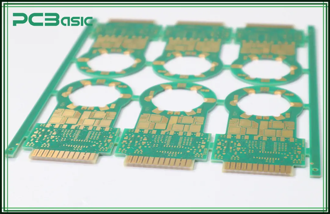
The printed circuit board (PCB) is the core part of electronic equipment, like the "heart" of a device. It not only provides support for the electronic components, but also connects them together through conductive copper pathways, which we call "trace". These traces allow current to flow freely through the circuit, ensuring each component to perform its specific function.
As the foundation of electronic systems, PCB plays a vital role in electronic equipment. Therefore, let’s have an in-depth understanding of what circuit boards are made of and how they work, which can help us better understand their key role in electronic devices.
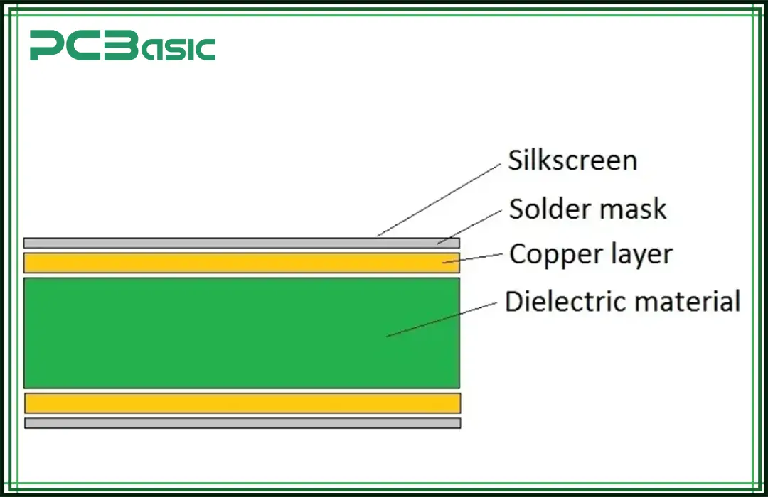
The selection of PCB materials is strict. They should have good insulating and conductive properties. For different layers of the board, the materials used are also different.
|
Layer |
Function |
Material |
|
Substrate |
Provides structural integrity and stability to the circuit board. |
Fiberglass or FR4 (flame-retardant material) |
|
Copper Foil |
Forms conductive pathways (traces) on the circuit board, allowing electrical current to flow. |
Copper |
|
Solder Mask |
Covers copper traces to protect them from oxidation and prevent short circuits. |
Epoxy or polymer (typically green) |
|
Silkscreen |
Prints symbols and labels on the solder mask for easier identification of components and connection points. |
Ink (white, yellow, or other colors) |
|
Other Materials |
Used in high-frequency PCBs, suitable for applications in radio communication and high-power distribution. |
Teflon, ceramics, or metal-core substrates |
These layers in the board work together to form a stable and reliable electronic platform. The choice of circuit board materials directly affects the performance of the PCB, including its current handling capacity, heat resistance and anti-interference to the external environment.
There are many types of circuit boards, and different types are suitable for different electronic devices. Understanding the types of circuit boards is crucial to PCB design and manufacturing. Here are a few common types of circuit boards:
• Single-layer PCB: This circuit board has only one layer of copper foil, simple structure, low cost, and is usually used for simpler electronic products.
• Double-layer PCB: The circuit board has copper foil on both sides, connected through small holes (called through-holes), making it suitable for devices with slightly more complex functions.
• Multi-layer PCB: It is composed of multiple layers of copper foil and insulating materials. It can handle more complex circuits and is suitable for high-performance equipment such as computer motherboards and medical equipment.
• Flexible PCB: It is made of flexible materials that can be bent, suitable for wearable devices, mobile phones and other products that need to be folded or moved.
• Rigid-Flex PCB: It combines the characteristics of rigid and flexible PCB, both stable and flexible, suitable for electronic equipment with complex structure.
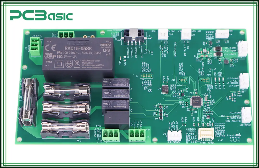
PCBs work by directing the electrical signal through the correct pathway, enabling the flow of electricity. As the current passes through the PCB, copper traces transfer the current from one component to another, such as resistors, capacitors, and integrated circuits (ICs), to complete their specific function. In a smartphone, for example, PCBs connect the screen, battery, camera, and other components to ensure smooth operation of it.
In multilayer PCBs, copper traces are stacked on different layers, which makes circuit design more complex. This is critical for those space-constrained but performance-demanding devices such as computers and telecommunications equipment.

An excellent PCB needs both precise design and advanced PCB manufacturing techniques. From creative printed circuit board design to ultimate operable physical circuit board, designers use tools and software to carefully build circuit diagrams and layouts to ensure that each component works efficiently.
After designing, these designs are transformed into actual circuit boards with the help of precise manufacturing techniques.
Next, let’s dive into the PCB design and fabrication process to understand how PCBs are made.
If you are curious about how to make a PCB, you need to understand its design first. From the initial conception of the circuit to the creation of a detailed layout, PCBs’ design involves multiple steps.
The first step in the PCB manufacturing process is the PCB design process. Here are the main PCB design steps:
Circuit Design: The first step in circuit board design is to design electronic circuits. Engineers use specialized software to create circuit diagrams, which show the different electronic components and the connections between them.
Component Selection: According to the needs of the designed circuit, designers need to choose the appropriate electronic components, such as resistors, capacitors and integrated circuits.
PCB Layout Design: Layout design is a key step in converting circuit diagrams into physical ones. In this process, design engineers use PCB design software to wisely arrange the component layout on the virtual circuit board. At the same time, they route copper traces that will connect the components. This process is critical to PCB performance and manufacturing quality.
Design Rule Check (DRC): After the layout design is completed, it needs to be DRC checked to ensure that the design meets all manufacturing standards. The check should ensure that the traces are properly spaced, components fit within the board, and there are no electrical conflicts.
Gerber File Generation: After finishing the whole design, export it as a Gerber file. It contains all the information needed for PCB manufacturing, including copper layer patterns, drill hole locations and component placements.
Only when the design is finished, the actual PCB manufacturing process begins. Here’s how circuit boards are made:
• Substrate Preparation: The first step of PCB manufacturing is to cut large sheets of the substrate material to the required sizes and shapes, which are mainly based on the design requirements of the final PCBs.
• Copper Foil: After the substrate is cut, applying a very thin layer of copper foil to its surface. This layer is adhered to the substrate by physical or chemical means and will become the conductive circuit on the PCB.
• Imaging: In this step, convert the circuit design into an image file first. Then, applying a special photosensitive material (photoresist) to the copper foil-covered substrate surface. After that, the circuit design pattern is transferred to the board by exposure technology. In this way, using ultraviolet irradiation through a mask to selectively expose certain areas of the board. The illuminated area hardens and the unexposed part remains soft. We often use a developer to remove the soft resist and expose the copper foil part that needs to be processed.
• Etching: In this key process, we remove unnecessary copper through chemical etching, such as ferric chloride or sulfuric acid. Time and accuracy of etching are very important. Too much or too little etching can affect the quality and performance of the circuit.
• Drilling: Precision drilling equipment can drill through holes in the circuit board. These holes are used to connect the different levels of the circuit and provide installation locations for components. Their accuracy is extremely important because even a hole misalignment can cause the board to not work properly.
• Plating: The plating process, usually with copper plating, is performed on drilled through holes. In this step, a layer of copper is covered to the hole walls, creating a conductive path between different layers. This process ensures an electrical connection between the through-hole and the plate layers, allowing signals to be transmitted between the layers.
• Solder Mask Application: Solder mask, also known as solder resist layer, is a green or other color protective coating that covers the copper traces to protect them from oxidation and short circuits during soldering. It also prevents solder from spilling into unwanted areas during the assembly process.
• Silkscreen Printing: The Silkscreen layer is printed on the surface of the PCB. It is used to indicate component labels, identifiers, and other information, which can help technicians to easily identify the location and function of each component during assembly, avoiding assembly errors.
• Final Test: After a PCB manufacturing is finished, it must pass a series of electrical tests, including flying probe and functional tests. These tests check for all shorts, open circuits, and overall electrical performance. If there are any defects on the board, the entire circuit system may fail. Therefore, testing is a key step to ensure the quality of the product.
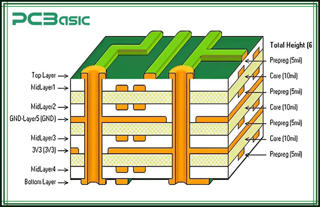
Multilayer PCB manufacturing is more complex than single-layer PCB production as they contain additional copper and insulating layers. The multilayer PCB manufacturing process is similar to that of a single layer, but the following steps are added:
• Layer Alignment and Stacking: When making a multilayer PCB, each layer of the circuit is ensured by an interlayer alignment device. Optical alignment systems are often used to ensure that all layers remain consistent after stacking. These layers are then pressed together using a laminator, which uses high temperature and high pressure to make the layers firmly bonded while ensuring electrical performance.
• Copper foil covering: For multilayer PCBs, the copper foil covers both sides of the substrate.
• Segment Stacking: In some cases, the board needs to be stacked and pressed in stages, with each stage dealing with a different layer.
Multilayer PCBs are widely used in high-performance equipment such as computers, medical equipment and aerospace. Their complex structure allows them to achieve more functions in a limited space. Therefore, multilayer PCB design and manufacturing require precision machinery and PCB manufacturing equipment to ensure quality and functionality.
Choosing a reliable PCB manufacturer is very important for the quality of the circuit board. So why choose PCBasic? Mainly because PCBasic has the following advantages:
Choosing PCBasic for your PCB design and fabrication ensures top-quality results, professional service, and excellent value for your investment.
From an original fiberglass board to a fully functional printed circuit board, the PCB manufacturing process is quite complex. Every step, whether it is PCB design and fabrication or material selection and PCB production, is key to ensuring that the board functions properly. PCB manufacturing equipment and machines help engineers and technicians produce these complex components with precision and reliability.
Whether single-layer PCBs or complex multilayer designs, circuit boards form the basis of our modern electronics world. Understanding how circuit boards are made helps us better understand the engineering marvels behind the devices we rely on every day.
By exploring PCB design steps, the PCB manufacturing process, and understanding circuit board material, you now have a detailed overview of how to make a PCB and how circuit boards are made.
Assembly Enquiry
Instant Quote
Phone contact

+86-755-27218592
In addition, we've prepared a Help Center. We recommend checking it before reaching out, as your question and its answer may already be clearly explained there.
Wechat Support

In addition, we've prepared a Help Center. We recommend checking it before reaching out, as your question and its answer may already be clearly explained there.
WhatsApp Support

In addition, we've prepared a Help Center. We recommend checking it before reaching out, as your question and its answer may already be clearly explained there.