Global high-mix volume high-speed PCBA manufacturer
9:00 -18:00, Mon. - Fri. (GMT+8)
9:00 -12:00, Sat. (GMT+8)
(Except Chinese public holidays)
Global high-mix volume high-speed PCBA manufacturer
9:00 -18:00, Mon. - Fri. (GMT+8)
9:00 -12:00, Sat. (GMT+8)
(Except Chinese public holidays)
HomePage > Blog > Knowledge Base > Circuit Board Patterns: Design, Types, and Applications
Modern electronic products all require efficient and precise circuit board pattern design and layout. Whether it is a smartphone, a laptop, a high-speed communication system or an industrial control system, a well-designed circuit board pattern can ensure the smooth transmission of electrical signals, the stable distribution of power, and the normal operation of all components. The circuit board pattern is the wiring scheme of electronic components and conductive pathway, which is the basis for ensuring circuit performance, anti-interference ability and product reliability.
As electronic devices become smaller, faster and more complex in structure, the design requirements for circuit board patterns are also getting higher and higher. It not only needs to ensure the correct electrical connection, but also take into account issues such as signal integrity, electromagnetic compatibility (EMC), power distribution and heat dissipation. Designers usually use professional tools such as Altium and Eagle to complete the design of circuit patterns from circuit diagrams to PCB layouts.
This article will introduce the circuit board pattern in detail, including its definition, working principle, common types, and design specifications, as well as its applications in fields such as network communication, radio frequency, and consumer electronics. Mastering this knowledge can help you design and manufacture high-performance and highly reliable electronic products.
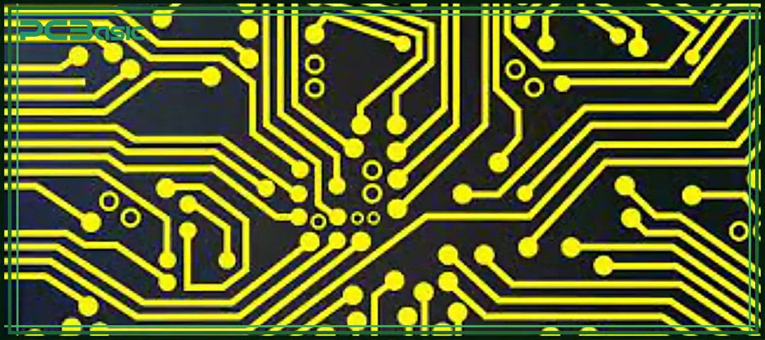
The circuit board pattern refers to the layout and functional design of components and conductive pathways on a printed circuit board (PCB). A circuit pattern is composed of copper trace, pad, via and some geometric shapes, which is used to define how electrical signals and power travel across the circuit board.
The circuit board pattern itself does not contain actual components or conductive materials, but it is an important blueprint for circuit board production. It determines where each component is placed, how the traces connect the components and the flow paths of signals and power in the circuit.
Designing a good circuit board pattern can help ensure signal integrity, reduce electromagnetic interference (EMI), rationally allocate power supply, and facilitate the layout and installation of components. Designers usually use professional tools such as Altium, Eagle and KiCAD to convert circuit schematic diagrams into manufacturable PCB patterns.
There are various types of circuit board patterns. Different patterns are applicable to different electronic products, meeting different circuit complexities and functional requirements. The following are several common types of circuit board patterns:
Single-Sided Circuit Board Pattern
The single-sided circuit pattern is the simplest one. All the conductive copper traces and components are concentrated on one side of the circuit board. This kind of circuit board has a simple structure, low cost and is easy to manufacture. It is widely used in toys, remote controls, calculators and other simple electronic products. This type of circuit board pattern is suitable for applications with low cost and low complexity.
Double-Sided Circuit Board Pattern
The circuit board pattern of a double-sided circuit board has conductive traces distributed on both the top and bottom layers of the circuit board. These two layers are connected by via or plated through holes. Compared with single-sided boards, it can hold more components, and the circuit layout is also more flexible. It is applicable to devices that require circuits of medium complexity, such as computer peripherals and home audio systems. Although double-sided boards are a bit more complex, the cost increase is not significant, and thus they are widely used.
Multilayer Circuit Board Pattern
The multilayer circuit board pattern is composed of 4 or more layers of copper traces, with insulating materials separating each layer. The inner layers are mainly used for signal routing and power distribution, while the outer layers are used for component mounting. This kind of PCB pattern supports high-density and high-complexity circuit design and is suitable for high-end electronic products such as smartphones, tablet computers and high-speed communication devices. Multilayer boards are more difficult to manufacture and have a higher cost, but they can meet the requirements of complex circuits.
Power Plane Pattern
The power plane circuit pattern is specifically used for power distribution. A large area of copper plane is laid on the circuit board to form a low-impedance power path. This helps to provide a stable voltage, reduce power supply noise, enhance heat dissipation effect and improve signal integrity at the same time. This kind of pattern is usually used in high-speed digital circuits and high-power devices.
Ground Plane Pattern
The ground plane circuit board pattern also uses a large copper plane as a unified ground reference. The ground layer can effectively shield signals, prevent electromagnetic interference (EMI), and enhance the stability of the entire circuit board. The ground layer is very common in multilayer boards and is usually used together with the power layer.
Differential Pair Circuit Pattern
In this circuit board pattern, two copper traces are routed in parallel and transmit signals with equal amplitudes but opposite directions. This layout can significantly enhance the anti-interference ability, reduce the influence of noise, and ensure timing accuracy. The differential pair circuit pattern is often used in the circuit design of high-speed digital signals and high-frequency analog signals, such as USB, HDMI, and Ethernet high-speed interfaces.
Clock Distribution Circuit Pattern
This kind of PCB pattern is used to efficiently distribute clock signals, ensuring that all clock-related components in the circuit can work synchronously. Clock distribution is particularly crucial for high-speed systems such as processors and network switching devices. Good clock routing can reduce clock skew and ensure proper system operation.
RF Transmission Line Pattern
The RF transmission line circuit pattern is specifically designed for RF and microwave circuits. The key point of this type of pattern is impedance matching, which reduces signal reflections and losses. It is widely used in devices such as wireless communication, radar, and radio frequency modules that require high-frequency signals. Special attention should be paid to the width, spacing and routing when designing.
Flexible and Rigid-Flex Circuit Board Patterns
Flexible PCB patterns are made of flexible materials such as polyimide and can be bent. They are used in applications that require flexibility, such as medical devices and wearable devices. Rigid-flex circuit board patterns combine rigid and flexible sections to achieve complex routing in a compact space and improve reliability. This type of board is widely used in high-demand fields such as aerospace, military industry and medical care.
 About PCBasic
Time is money in your projects – and PCBasic gets it. PCBasic is a PCB assembly company that delivers fast, flawless results every time. Our comprehensive PCB assembly services include expert engineering support at every step, ensuring top quality in every board. As a leading PCB assembly manufacturer, we provide a one-stop solution that streamlines your supply chain. Partner with our advanced PCB prototype factory for quick turnarounds and superior results you can trust.
A circuit board pattern is like a map for how current flows in a PCB. It decides where the current comes from, where it goes, and how it moves. Electrons come from the power source, flow along the path designed in the circuit pattern, pass through different components, and then return to the power source, forming a complete circuit.
In this process, the copper trace works like a highway for the current. It carries the current from one component to another. The pad is the place where a component connects. It provides a fixed and conductive point for the pins of resistors, capacitors, ICs, and other parts, making soldering and connection easy. In multilayer PCBs, the via acts like a bridge. It helps signals move between different layers so the board can have complex routing and higher density.
If the circuit board pattern is broken, damaged, or not designed well, it can cause an open circuit, and the current will stop flowing. The circuit will not work. On the other hand, if there is an accidental direct path between the positive and negative sides of the power supply (or between power and ground) without passing through the load, that is a short circuit. A short circuit lets the current skip the components and go straight back to the power source. This can cause the power supply to overload, heat up, damage parts, or even cause a fire.
To prevent these problems, circuit designs usually include protection devices like a fuse or a circuit breaker. These parts can cut off the circuit in time when an abnormal current happens, protecting the PCB and connected equipment.

Designing a reliable circuit board pattern requires good planning, following engineering standards, and considering electrical performance, manufacturing process, and long-term reliability. Below are important guidelines for designing a circuit board pattern:
Electrical Connectivity
The first task of a circuit board pattern is to ensure stable and reliable electrical connections between components. This requires precise component placement and reasonable copper trace routing to safely carry current from one component to another. The routing should reduce resistance and energy loss as much as possible to avoid failures or performance problems caused by poor connections.
Signal Integrity
A good circuit pattern keeps electrical signals stable and clear. The design should use controlled impedance traces, match trace lengths, and separate high-frequency or sensitive signals to prevent crosstalk. These methods ensure signals travel across the board without distortion, meeting the needs of high-speed or high-accuracy circuits.
EMI Control
A circuit board pattern should include ground planes and shielding and follow EMC standards to reduce electromagnetic interference (EMI). This helps prevent outside electromagnetic waves from affecting the circuit and stops the circuit from creating too much interference itself. The goal is to make sure the device works reliably in different environments.
Power Distribution
A good PCB pattern should have well-designed power planes and decoupling capacitors to give each component a stable power supply. Power routing should be as even and low-impedance as possible to lower noise and voltage changes, improving circuit performance and reliability.
Component Placement
The circuit board pattern should have a logical component placement. Related components should be placed close together to shorten signal paths and improve circuit performance. There should also be enough space between components for heat dissipation, inspection, and maintenance. Good placement also helps with easier manufacturing and assembly.
Routing Efficiency
An efficient circuit pattern should use short, direct traces and avoid unnecessary bends to reduce signal delay and power loss. The via positions should be well planned so they don’t block routing. For high-speed signals, differential pair routing should be used to improve noise immunity and keep signal integrity.
Design for Manufacturability
A good PCB pattern is not just well-designed but also easy to produce. The design should consider manufacturing limits, such as minimum trace width, pad size, and clearance, to make sure it fits the factory’s capabilities. This helps reduce defects and rework.
Thermal Management
In a circuit board pattern, thermal management should be part of the design. For example, add thermal vias, copper pours, and heat sinks near hot components. These help the board release heat, prevent local overheating, and improve the stability and lifespan of the circuit.
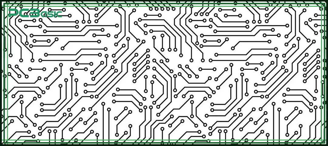
To build a complete circuit board, every step from design to production must be accurate and well-organized. Here are the common steps:
First, decide what components the circuit needs and determine the values for each one. For example, if you are designing a regulated DC power supply, you might need a 7805 regulator, a transformer, and filter capacitors. The design should select the right parts and circuit structure based on the required function.
Use software like Altium or Eagle to draw the circuit schematic. After finishing the schematic, use the software to create the circuit board pattern layout, which defines the trace routes and component positions on the PCB. Pay attention to trace direction, component placement, grounding, and power distribution to ensure the circuit works well and can be manufactured easily.
Use simulation software like Multisim to test the circuit and check if it works as expected. This helps verify whether the circuit pattern design meets the requirements. Problems can be found and fixed early, saving materials and time.
Once the design is confirmed, you can start making the PCB. First, print the PCB pattern onto copper-clad material. Then, use etching to remove the unwanted copper, leaving only the circuit pattern. Finally, solder the components onto the board. Testing and tuning may also be needed to make sure the circuit board works properly.
When designing a PCB, it is necessary to be clear about the difference between the circuit board pattern and the footprint. Although these two terms are sometimes confused, their roles in design are completely different.
Footprint refers to the physical size and mounting position design of a component on the PCB. It includes details like the pad shape, hole locations, and silkscreen outline, which guide how the component is placed correctly on the board. The purpose of the footprint is to make sure the component is installed in the right spot on the PCB and aligns accurately with the pads for easy soldering. A good footprint design not only improves production efficiency but also ensures soldering quality and the mechanical stability of the final product. It is an essential part of PCB design.
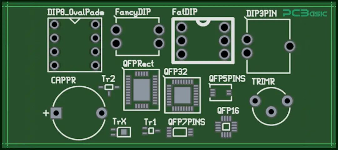
Core differences:
|
Circuit Board Pattern |
Footprint |
|
Defines signal routing and electrical connections |
Defines component mounting locations |
|
Focuses on connectivity and signal integrity |
Focuses on mechanical placement accuracy |
|
Critical for EMI control and power delivery |
Critical for soldering and assembly |
The circuit board pattern is the basis of modern electronic products. It determines how each component is connected together and how it works. Whether it is a single-sided circuit board used in simple equipment or a complex multilayer PCB used in telecommunication equipment, the design of the circuit board pattern is of great significance. If well designed, the circuit board will not only have good performance but also be more reliable and easier to produce.
As long as engineers follow the norms during the design process, combine the actual needs and use the right design tools, they can produce high-quality circuit boards. Whether it is creating works of interest or designing advanced communication equipment, learning to design circuit board graphics is the key to success.

Assembly Enquiry
Instant Quote
Phone contact

+86-755-27218592
In addition, we've prepared a Help Center. We recommend checking it before reaching out, as your question and its answer may already be clearly explained there.
Wechat Support

In addition, we've prepared a Help Center. We recommend checking it before reaching out, as your question and its answer may already be clearly explained there.
WhatsApp Support

In addition, we've prepared a Help Center. We recommend checking it before reaching out, as your question and its answer may already be clearly explained there.