Global high-mix volume high-speed PCBA manufacturer
9:00 -18:00, Mon. - Fri. (GMT+8)
9:00 -12:00, Sat. (GMT+8)
(Except Chinese public holidays)
Global high-mix volume high-speed PCBA manufacturer
9:00 -18:00, Mon. - Fri. (GMT+8)
9:00 -12:00, Sat. (GMT+8)
(Except Chinese public holidays)
HomePage > Blog > Knowledge Base > Ceramic PCBs – A Complete Guide
Most traditional circuit boards use FR4 or epoxy resin as the base material, which is suitable for ordinary consumer electronic products. However, they often fail to withstand high-power and high-frequency conditions. To solve these problems, engineers began to choose ceramic PCBs.
A ceramic circuit board is not a simple alternative to the ordinary PCB, but a more advanced technology. It has excellent thermal conductivity, electrical insulation and dimensional stability. In other words, ceramic substrate PCBs can still operate stably and reliably in high-temperature, strong vibration or corrosive environments, making them highly suitable for fields such as aerospace, defense, automotive electronics, medical equipment and 5G communications.
In this comprehensive guide, we will take you through a thorough understanding of ceramic PCB: what it is, its features, commonly used materials and types, specific application scenarios, manufacturing processes, and the differences between it and FR4 and MCPCB.
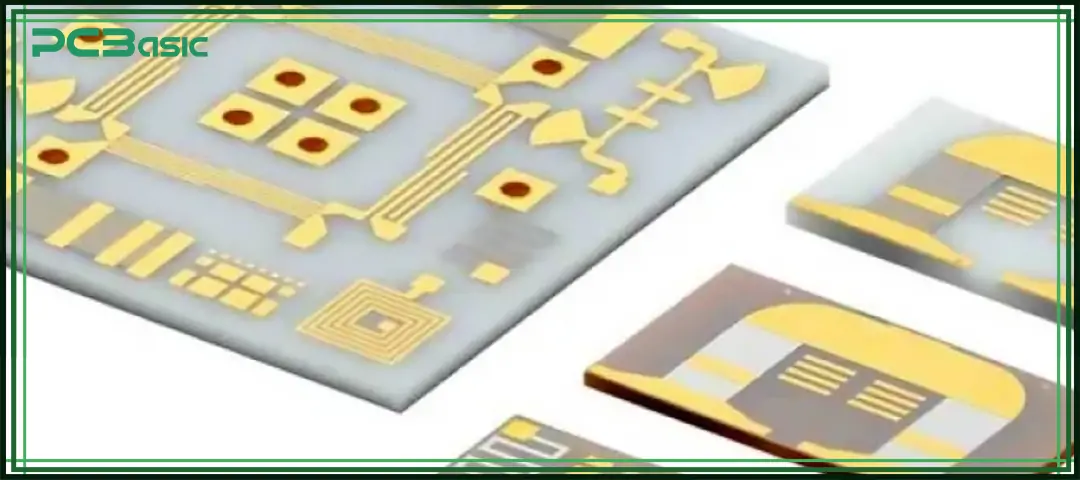
A ceramic PCB is a special type of printed circuit board. Its substrate is not made of traditional fiberglass epoxy resin (FR4), but advanced ceramic materials such as alumina (Al₂O₃), aluminum nitride (AlN), beryllium oxide (BeO), silicon carbide (SiC) or boron nitride (BN). Ceramics are used instead of organic materials; ceramic circuit boards possess properties that ordinary circuit boards do not have, such as thermal conductivity, electrical insulation, and chemical corrosion resistance.
It is precisely because of these characteristics that ceramic substrate PCBs are widely used in high-power electronics, RF and microwave systems, aerospace, defense equipment, automotive power modules, LED lighting and other applications that require high reliability.
Unlike an MCPCB (metal core circuit board), which relies on metal layers to assist with heat dissipation, a ceramic PCB itself integrates high thermal conductivity directly into its substrate. This means that it usually does not require additional heat sinks, the system design is simpler, and it can also support smaller and higher-density circuits.
In simple terms, the ceramic PCB is not merely a substitute for FR4, but rather a more advanced new-generation circuit solution. It can maintain stable operation in high-temperature, high-frequency and corrosive environments, while providing long-term reliability in critical applications.
The performance of ceramic PCBs mainly stems from the following prominent features:
The most notable feature of a ceramic PCB is its fast heat dissipation. The thermal conductivity of a common FR4 circuit board is only about 0.3 W/m·K, while that of alumina oxide (Al₂O₃) can reach 20-30 W/m·K, and that of aluminum nitride (AlN) even exceeds 200 W/m·K. This means that the heat of the ceramic circuit board can dissipate 20 to 100 times faster than that of traditional boards, effectively avoiding overheating of components and enhancing reliability.
A ceramic PCB substrate has excellent electrical insulation. Materials such as alumina and aluminum nitride have low dielectric loss and stable dielectric constants, which can reduce signal leakage. This makes ceramic PCBs an ideal choice for radio frequency (RF), microwave and high-speed digital circuits, ensuring stable and reliable signals.
Ceramic PCBs hardly expand under temperature changes, and their coefficient of thermal expansion (CTE) is close to that of silicon chips. This reduces the stress of thermal cycling on circuit boards and chips, making ceramic substrate PCBs highly reliable in semiconductor packaging.
Ceramic PCBs have a strong structure and can withstand vibration, shock and mechanical stress. This durability is of great significance in fields such as aerospace, automotive electronics and defense electronics.
Unlike FR4 or some MCPCBs, ceramic substrate PCBs can resist corrosion from chemicals, solvents and moisture. This enables ceramic PCBs to be safely used in harsh environments such as medical equipment, industrial automation and energy.
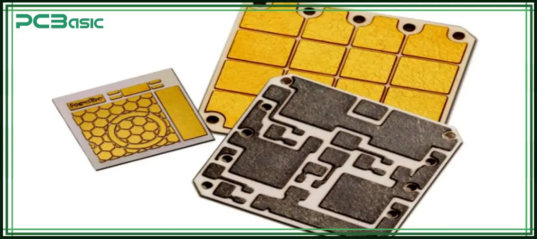
In industrial PCB design, the selection of substrate materials directly affects the performance of the circuit board. Different ceramic materials have their own unique thermal conductivity, mechanical properties and electrical performance, and thus are suitable for various types of electronic applications.
The following table lists several common ceramic PCB materials, along with their thermal conductivity, main features and typical applications, serving as a reference for design and material selection.
|
Material |
Thermal Conductivity (W/m·K) |
Features |
Typical Applications |
|
Alumina (Al₂O₃) |
18–35 |
Affordable, reliable |
LEDs, consumer electronics, automotive circuits |
|
Aluminum Nitride (AlN) |
80–200+ |
High thermal conductivity, CTE close to silicon |
High-power electronics, aerospace systems, and MCPCB replacement in power modules |
|
Beryllium Oxide (BeO) |
209–330 |
Exceptional thermal conductivity, but toxic |
Military and aerospace ceramic PCB substrates |
|
Silicon Carbide (SiC) |
120–270 |
Excellent electrical and thermal properties |
High-power RF and power device ceramic PCBs |
|
Boron Nitride (BN) |
3.3–4.5 |
Lightweight, chemically stable, low dielectric constant |
RF circuits, heat-spreader ceramic PCBs |
|
Category |
Type |
Key Features |
Typical Applications |
|
Fabrication |
HTCC (High-Temperature Co-fired Ceramic PCB) |
Sintered at 1600–1700 °C; uses tungsten or molybdenum conductors; highly durable and reliable; higher cost |
High-performance electronics |
|
LTCC (Low-Temperature Co-fired Ceramic PCB) |
Sintered at 850–900 °C; uses glass and gold/silver pastes; less warpage, stable |
RF modules, LED lighting, miniaturized electronics |
|
|
Thick Film Ceramic PCB |
10–13 μm silver, gold, or palladium conductive layer; prevents copper oxidation; reliable in harsh environments |
General high-reliability ceramic circuit boards |
|
|
Thin Film Ceramic PCB |
Nano-scale conductive/insulating thin layers; supports high-precision circuits |
High-precision RF and microwave circuits, compact designs |
|
|
Structure |
Single-layer Ceramic PCB |
Simple structure; efficient heat dissipation |
Power modules, LED applications |
|
Multilayer Ceramic PCB |
Stacked ceramic substrates; supports high-density interconnections |
Miniaturized circuits, complex electronic designs |
|
|
Advanced Variants |
LAM (Laser Activation Metallization) |
Laser bonds copper tightly to ceramic; durable and reliable |
High-performance electronics |
|
DPC (Direct Plated Copper) |
Vacuum sputtering + electroplating; thin, precise copper layer |
High-frequency electronics |
|
|
DBC (Direct Bonded Copper) |
Thick copper (140–350 μm) bonded to ceramic |
High-current power modules |
Time is money in your projects – and PCBasic gets it. PCBasic is a PCB assembly company that delivers fast, flawless results every time. Our comprehensive PCB assembly services include expert engineering support at every step, ensuring top quality in every board. As a leading PCB assembly manufacturer, we provide a one-stop solution that streamlines your supply chain. Partner with our advanced PCB prototype factory for quick turnarounds and superior results you can trust.
The versatility of the ceramic PCB makes it essential in many industries:
• LED Lighting: High-power LEDs benefit from ceramic substrates that eliminate the need for heat sinks.
• Automotive Electronics: Used in ECUs, power management, and EV modules where vibration and heat are challenges.
• Aerospace & Defense: Radar modules, missile guidance, avionics – reliable ceramic circuit boards under extreme conditions.
• Telecommunications: RF amplifiers, microwave circuits, and 5G infrastructure rely on ceramic PCB substrates for signal integrity.
• Medical Devices: Implantables and diagnostic equipment need biocompatible and chemically resistant ceramic PCBs.
• Industrial Power Electronics: Inverters, converters, and renewable energy systems benefit from high-power ceramic substrate PCBs.
• Semiconductor Packaging: Chip carriers and hybrid microelectronics use multilayer ceramic circuit boards for high density and thermal control.
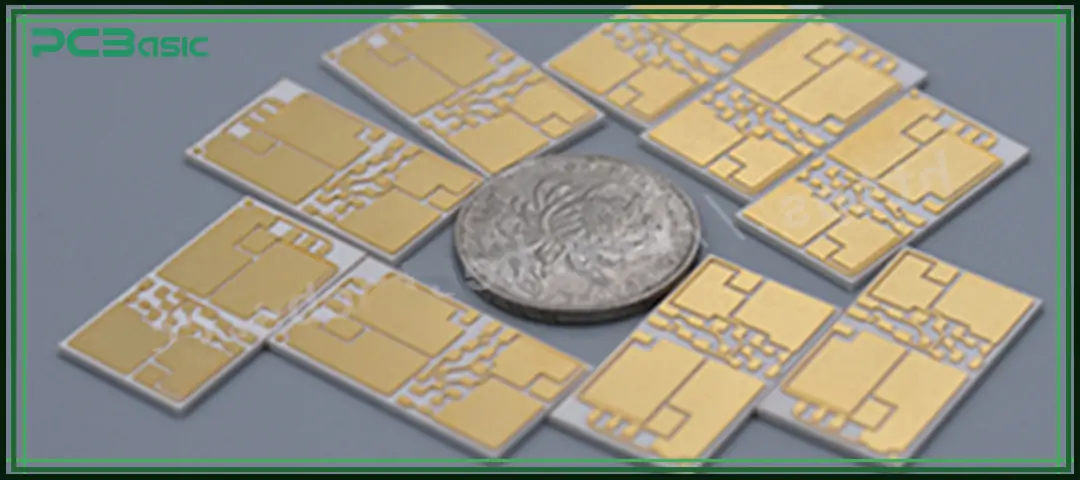
Manufacturing a ceramic PCB is not a simple process. It involves multiple professional steps, each of which affects the performance and reliability of the final circuit board.
First, use CAD software for circuit design. Engineers will particularly consider the heat dissipation requirements and high-frequency signal transmission performance of ceramic PCBs to ensure that the circuit layout is both reasonable and reliable.
Cut the ceramic substrate materials (common ones include Al₂O₃ and AlN) into required sizes, and then polish and clean them. This step is to ensure that the substrate surface is flat, free of dust and impurities, facilitating subsequent processes.
Conductive pastes such as silver (Ag), gold (Au), and copper (Cu) are printed on the surface of ceramic substrates to form circuit traces. The thin-film process can also deposit finer conductive layers, making it suitable for high-precision circuits.
Use laser or mechanical drilling to create vias through the substrate. Then, metallization treatment is carried out inside the hole to establish reliable interconnections between circuit layers.
If it is a multilayer ceramic PCB, the multilayer substrates will be precisely aligned and laminated together to form a multilayer structure. This can support high-density interconnections and more complex circuit designs.
The laminated ceramic substrate is placed in a high-temperature furnace and sintered at 850 to 1700 °C to firmly bond the ceramic and metal layers, ensuring the stability and strength of the circuit board.
ENIG, ENEPIG, immersion silver, or immersion tin are carried out on the surface of the circuit board. These treatments can enhance the solderability performance and prevent the copper layer from oxidizing.
Install surface-mount devices (SMDs) on the circuit board to complete the basic circuit functions. After that, electrical tests and thermal reliability tests will also be carried out to ensure that the ceramic PCB can work normally.
The final step is to cut or V-score the circuit board to complete the shape processing. Qualified finished products will be packaged and prepared for shipment by the ceramic PCB manufacturer.
|
Feature |
FR4 PCB |
MCPCB |
Ceramic PCB |
|
Thermal Conductivity |
~0.3 W/m·K |
1–5 W/m·K |
20+ W/m·K |
|
Cost |
Low |
Medium |
High |
|
Mechanical Strength |
Good |
Excellent |
Brittle |
|
Applications |
General electronics |
LEDs, automotive, power |
Aerospace, RF, high power |
• FR4: inexpensive but poor at heat dissipation.
• MCPCB: balance of cost and performance.
• Ceramic PCB: superior thermal conductivity, but very expensive.
Ceramic PCBs are the key choice for high-performance electronic assembly. It combines high thermal conductivity, excellent electrical performance, durability and chemical corrosion resistance, and is thus becoming increasingly important in fields such as aerospace, automobiles, telecommunications, defense, LED and medical equipment.
Although ceramic PCBs are more expensive than FR4 or metal core PCBs and are more fragile, they can enhance long-term reliability, reduce heat dissipation requirements, thereby extending the service life of electronic products, and overall save costs.
Assembly Enquiry
Instant Quote
Phone contact

+86-755-27218592
In addition, we've prepared a Help Center. We recommend checking it before reaching out, as your question and its answer may already be clearly explained there.
Wechat Support

In addition, we've prepared a Help Center. We recommend checking it before reaching out, as your question and its answer may already be clearly explained there.
WhatsApp Support

In addition, we've prepared a Help Center. We recommend checking it before reaching out, as your question and its answer may already be clearly explained there.