Global high-mix volume high-speed PCBA manufacturer
9:00 -18:00, Mon. - Fri. (GMT+8)
9:00 -12:00, Sat. (GMT+8)
(Except Chinese public holidays)
Global high-mix volume high-speed PCBA manufacturer
9:00 -18:00, Mon. - Fri. (GMT+8)
9:00 -12:00, Sat. (GMT+8)
(Except Chinese public holidays)
HomePage > Blog > Knowledge Base > PCB Test Points – A Complete Guide
In modern electronic products, every printed circuit board testing process cannot do without reasonably designed test points to verify the quality and functionality of the circuit. Engineers should not only focus on circuit layout and performance when designing, but also consider design for testing from the very beginning. The key among them is to add PCB test points.
Whether in the prototype development stage or in mass production, PCB test points are important interfaces for printed circuit board assembly test, debugging and quality control. If there are no properly arranged SMD test points, the production line will become inefficient, troubleshooting will be more complicated, and the risk of undetected errors may also increase.
This article will combine industry experience to comprehensively introduce the role of PCB test points - covering their definitions, importance, types, design specifications, limitations and best practices, helping engineers achieve reliable printed circuit board testing in all production stages.

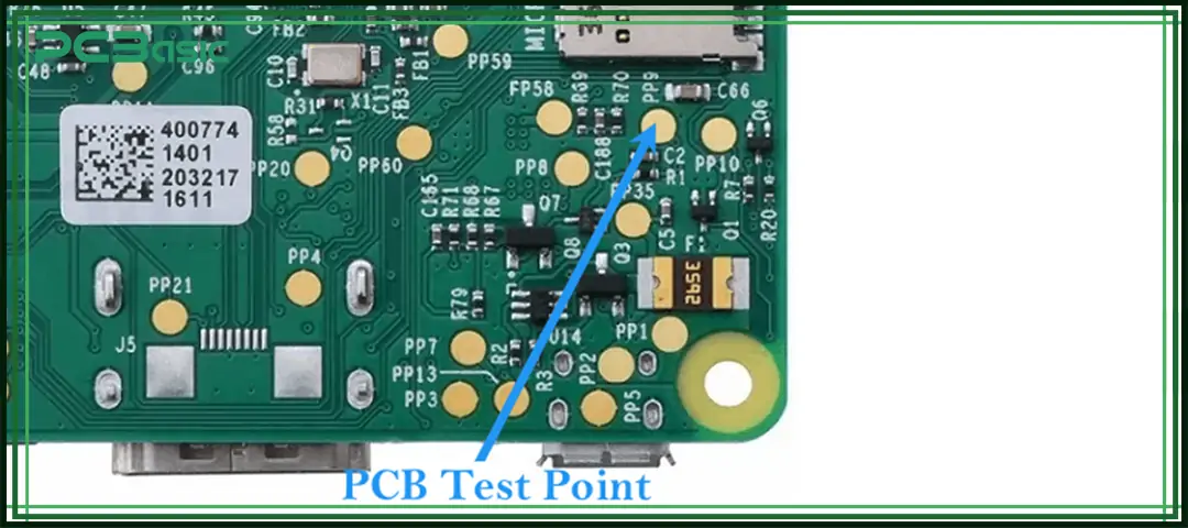
A PCB test point is a specially designed exposed copper area on the outer layer of a circuit board, used to directly connect to a specific net in the circuit. In simple terms, it is a small pad, via, plated through-hole, or wire loop through which test probes can contact the circuit board without modifying the design or removing components.
These circuit board test points are the positions where the probes come into contact. Technicians and automated equipment can measure voltages and check continuity here, or inject signals in the printed circuit board testing. Through these operations, we can quickly and reliably verify the performance of the circuit board at different stages of manufacturing and debugging.
To ensure mechanical strength, PCB test points are typically made of phosphor bronze and often with a silver-plated coating to improve electrical conductivity. Meanwhile, for ease of identification, many PCB test points will be labeled with the net name or reference symbol on the silkscreen, such as "GND" or "PWR".

Time is money in your projects – and PCBasic gets it. PCBasic is a PCB assembly company that delivers fast, flawless results every time. Our comprehensive PCB assembly services include expert engineering support at every step, ensuring top quality in every board. As a leading PCB assembly manufacturer, we provide a one-stop solution that streamlines your supply chain. Partner with our advanced PCB prototype factory for quick turnarounds and superior results you can trust.
Adding PCB test points in circuit board design is a key step to ensure smooth progress and reliable results for the printed circuit board assembly test. Without reasonably designed test points, many problems may be overlooked during the production stage and only surface when the product enters the later stage. This not only makes maintenance difficult but also brings higher costs and risks.
• Ensure circuit functionality: Through PCB test points, power rails, ground nets and signal traces can be quickly measured at different stages of the circuit board to ensure that these key parts can work properly during and after production.
• Simplify debugging and repair: When a circuit board malfunctions, engineers can directly connect the probe to the circuit board test points to quickly identify the root cause of the problem without having to remove the components or cut off the traces. This not only increases the troubleshooting speed but also reduces the damage to the circuit board itself.
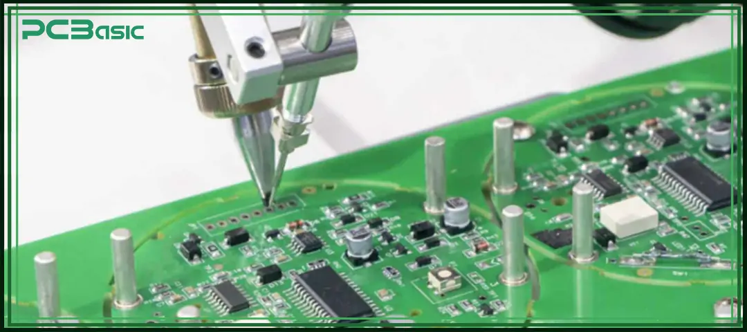
• Enable automation: In mass production, the properly distributed SMD test point pads can be perfectly coordinated with in-circuit testers or flying probe machines to achieve automated testing. This makes the testing speed of batch products faster and the accuracy higher.
• Reduce cost and time: Without early detection, problems may not be discovered until the entire board assembly is completed. At this point, the cost of rework is extremely high, and in some cases, the entire board may even need to be scrapped. By identifying and solving problems in advance through test points, this situation can be effectively avoided, saving a great deal of time and cost.
• Support prototypes and mass production: Whether it is a small-batch prototype in the R&D stage or large-scale mass production in the factory, PCB test points play an important role. In prototype development, they help engineers verify design ideas. During the mass production stage, they ensure a stable and reliable production process.
Overall, well-designed PCB test points on a PCB can make testing and verification more efficient, not only helping manufacturers save costs and time, but also ensures the performance and quality of the circuit board, ultimately enhancing customer satisfaction.

In the process of PCB design and manufacturing, PCB test points are usually divided into two major types: one is the manual/probe test points that facilitate manual debugging by engineers, and the other type is the automated test points prepared for automated inspection in mass production.
Manual test points are the most common type of test points, mainly used in conjunction with handheld test devices, such as multimeters or oscilloscopes.
Manual test points usually appear as small pads, posts or wire loops, and are often labelled on the silkscreen (such as GND, VCC) to facilitate engineers or technicians to quickly find the corresponding signal or power line.
Manual test points enable testers to quickly verify the voltage, current and continuity of the circuit, thereby determining whether the circuit is functioning properly. They are very common in prototyping and PCB repair, as these stages often require frequent debugging and measurement.
Automated PCB test points are specifically designed for machine-based inspection. They are usually flat pads, vias or pins, and their sizes are compatible with the spring-loaded probes in fixtures or flying needle systems.
They are crucial in automated PCB testing methods, especially in:
• Bare board testing
• In-Circuit Testing (ICT)
• Flying Probe Testing (FPT)
Correctly designing PCB test points can ensure that they are both accessible and reliable during the testing process.
1. Try to place all test points on the PCB on the same side of the circuit board.
2. Circuit board test points should be evenly distributed to facilitate parallel probe testing.
3. Avoid placing test points underneath tall components.
4. When necessary, place the test points close to the edge of the circuit board to facilitate the contact of the probes.
|
Parameter |
Recommended |
Minimum |
|
Test point size |
0.050 inch |
0.035 inch |
|
Spacing (point-to-point) |
0.100 inch |
0.050 inch |
|
Point-to-component spacing |
0.100 inch |
0.050 inch |
|
Point-to-board edge spacing |
0.125 inch |
0.100 inch |
Most modern PCB CAD tools support design for testing (DFT) modules:
1. Define rules (size, spacing, grid, available layers).
2. Automatically select appropriate pads, vias, and pins.
3. Assign these candidate points as test points.
4. Use the Test Point Manager to verify whether the spacing meets the requirements.
5. Export the test point files for subsequent fixture production.
This design process can ensure that the PCB test points meet both the design and manufacturing requirements simultaneously.

Even simple test points on PCBs can fail if poorly implemented. Common errors include:
• Placing test points too close (<0.1 in), causing probe collision.
• Forgetting to assign them as test points in CAD (pads alone don’t count).
• Hiding test pads under tall or shielded components.
• Using pads too small for reliable probe contact.
• Adding stubs on high-speed signals, causing reflections.
• Overusing circuit board test points can increase the risk of shorts.
Avoid these pitfalls with strong DFT manufacturing practices.
Although PCB test points are small, they play a very significant role in printed circuit board testing. They enable engineers to access circuit nets quickly, accurately and reliably, and are a core part of modern PCB testing methods such as ICT and FPT.
As long as the layout is reasonable, the appropriate size is controlled, and the design for the testing process is combined in CAD, the maximum effect of the circuit board test points can be ensured. If common mistakes can be avoided and their limitations understood, the test results will be better.
Whether it is making prototypes or conducting large-scale DFT manufacturing, the test points on the PCB cannot be ignored. They are the key bridges connecting the design with the final high-quality product.
Q1: What size should test points be?
Ideally, 0.050 inches; minimum, 0.035 inches for reliable probing.
Q2: Can vias or through-holes be used as test points?
Yes. Vias and through-holes can function as circuit board test points, provided they are correctly assigned in CAD.
Q3: ICT vs. FPT — which should I choose?
• ICT: Best for mass production, very fast but costly fixtures.
• FPT: Flexible, low cost, slower—ideal for prototypes.
Q4: Do prototypes need test points?
Yes. Even in small runs, SMD test point pads help engineers debug quickly and save development time.
Q5: How to avoid shorts between test points?
Maintain spacing ≥0.1 in and limit unnecessary test points to reduce accidental shorts.

Assembly Enquiry
Instant Quote
Phone contact

+86-755-27218592
In addition, we've prepared a Help Center. We recommend checking it before reaching out, as your question and its answer may already be clearly explained there.
Wechat Support

In addition, we've prepared a Help Center. We recommend checking it before reaching out, as your question and its answer may already be clearly explained there.
WhatsApp Support

In addition, we've prepared a Help Center. We recommend checking it before reaching out, as your question and its answer may already be clearly explained there.