Global high-mix volume high-speed PCBA manufacturer
9:00 -18:00, Mon. - Fri. (GMT+8)
9:00 -12:00, Sat. (GMT+8)
(Except Chinese public holidays)
Global high-mix volume high-speed PCBA manufacturer
9:00 -18:00, Mon. - Fri. (GMT+8)
9:00 -12:00, Sat. (GMT+8)
(Except Chinese public holidays)
HomePage > Blog > Knowledge Base > Back Drilling in PCB Manufacturing
With the continuous development of electronic products towards higher speeds, smaller sizes and higher signal densities, engineers need to pay more and more attention to the issue of signal integrity when conducting PCB drilling and assembly.
One of the easily overlooked but very crucial factors is the via stub - it is the redundant part of the copper barrel segment in the plated through-hole that is not involved in signal transmission. These seemingly tiny metal segments can actually act like small antennas, causing signal reflection, ringing and resonance under high-frequency signals, thereby leading to signal distortion and degraded system performance.
Back drilling is precisely an effective process to solve this problem. By precisely removing these excess copper segments after the main drilling is completed, PCB back drilling can make the signal path cleaner and the impedance consistency more stable, thereby improving the reliability of high-speed circuits.
This article will start from the perspective of practical production, introduce the principle, process flow and key application of the back drilling in PCB manufacturing, and combine the manufacturing experience of PCBasic to help engineers better understand and apply this technology.
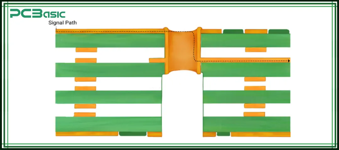
Back drilling, also known as controlled depth drilling (CDD), is a precise PCB drilling process used to remove unused copper barrels from through holes.
When a high-speed signal is transmitted through a plated through-hole in a multilayer board, the current only passes through a part of the copper wall, and the remaining unused copper is called a via stub. Although these copper stubs are conductive, they do not transmit signals. Instead, they will cause signal reflections at high frequencies, affecting signal quality.
Imagine that in a 12-layer circuit board, signals only need to connect from the first layer to the third layer, but the holes run through all 12 layers. Then, the part from the fourth layer to the twelfth layer 12 becomes an excess copper stub. These stubs will generate resonance and reflection when the frequency exceeds 3 GHz, seriously affecting signal integrity.
To avoid this situation, manufacturers will perform back drilling after the main drilling and plating steps. They use CNC equipment to re-drill holes from the opposite side of the circuit board with a slightly larger drill bit (generally about 0.2mm larger), and the drilling depth will be precisely controlled, stopping just before the signal layer.
In this way, the excess copper barrel can be removed without damaging the structure of the signal layer or insulation layer. Finally, what is obtained is a controlled-depth through hole with almost no remaining stubs, usually less than 10 mil (about 0.25 mm).
Through such PCB back drilling, high-speed signals can be transmitted more smoothly and stably between the layers of the circuit board, significantly improving the signal performance of the entire board.
In high-speed or high-frequency circuits, the signal transmission path within the circuit board must remain continuous and smooth. Once any discontinuity occurs, such as via stubs, it may cause signal reflection.
Simply put, a via stub is like a short open-ended transmission line. When a signal passes through, some of the energy is reflected back by this "dead-end" section. These reflections will trigger a series of issues:
• Cause impedance mismatch, making the signal bounce within the path and produce standing waves and energy loss;
• Lead to an increase in bit error rate (BER) in digital systems;
• Introduce jitter and crosstalk between differential pairs;
• Generate unwanted electromagnetic interference (EMI) that affects other circuits.
When the signal frequency exceeds several GHz, the length of the via stub sometimes approaches one-quarter of the signal’s wavelength. At this time, it becomes a resonant structure, making the reflection worse. Therefore, in applications such as 5G base stations, data center servers, automotive radar and high-speed backplanes, this problem must be solved through PCB back drilling.
By performing precise via drilling to shorten or even completely remove the extra stub, engineers can significantly reduce insertion loss, improve return loss, and keep the signal maintaining a more stable and predictable impedance consistency across critical signal paths.
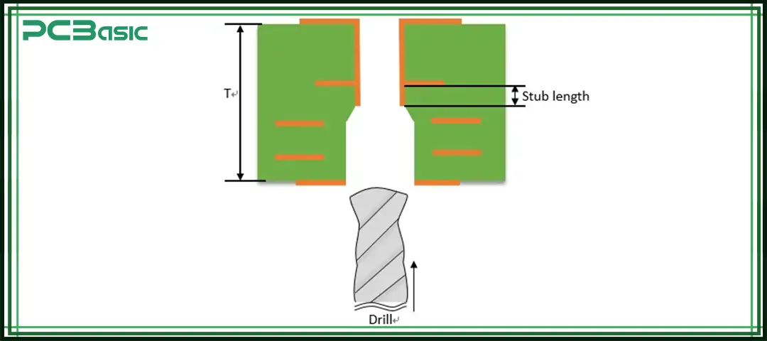
This section will systematically introduce the entire process of PCB back drilling from design, processing to inspection:
1. Standard Drilling and Plating
At the beginning of the entire PCB manufacturing process, standard PCB drilling is carried out first to create plated through holes (PTH). These holes are drilled completely through the board, and then a layer of copper is plated over the inner walls, forming a copper conductive barrel that can connect all the PCB layers.
2. Identify High-Speed Nets for Back Drilling
Next, design engineers will select vias that require back drilling. These vias are usually located on high-speed signal lines, such as differential pairs and clock lines.
3. Controlled-Depth Re-Drilling
When the electroplating is completed, the circuit board will be sent to the drilling station again for the actual back drilling. The factory will use CNC equipment with Z-axis depth control to re-drill from the opposite side of the board.
4. Cleaning and Inspection
After the back drilling is completed, the circuit board will undergo a thorough cleaning to remove debris and residue. Then, X-ray inspection or micro-section analysis is used to confirm the effect.
5. Final Finishing
After passing the inspection, the circuit board will enter the stages of solder mask, surface finish and assembly. At this point, the through holes processed by back drilling have been cleaned and tidied, with almost no residual stubs. It can make the signal transmission between multilayer boards smoother and more stable, while ensuring impedance consistency.
Time is money in your projects – and PCBasic gets it. PCBasic is a PCB assembly company that delivers fast, flawless results every time. Our comprehensive PCB assembly services include expert engineering support at every step, ensuring top quality in every board. As a leading PCB assembly manufacturer, we provide a one-stop solution that streamlines your supply chain. Partner with our advanced PCB prototype factory for quick turnarounds and superior results you can trust.
To achieve a consistent and reliable PCB back drilling effect, several key parameters must be clearly defined and strictly controlled during the design and manufacturing stages:
|
Parameter |
Typical Range |
Notes |
|
Drill Oversize |
+0.2 mm – 0.3 mm |
Ensures copper stub is fully removed |
|
Residual Stub Length |
≤ 10 mil (0.25 mm), ideally < 7 mil |
Shorter stub = better signal performance |
|
Depth Tolerance |
±0.10 mm – ±0.20 mm |
Depends on board thickness and machine accuracy |
|
Minimum Clearance |
≥ 0.2 mm |
Prevents the drill bit from damaging nearby planes |
|
Back Drill Direction |
Top, Bottom, or Both |
Determined by the signal entry layer |
|
Material Consideration |
FR-4, Rogers, or hybrid |
Different hardness affects drill speed |
|
Alternative Strategy |
Blind/Buried vias |
Used when stub removal is not feasible |
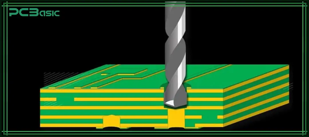
Modern back drilling relies on high-precision CNC PCB drilling machines. These devices are equipped with Z-axis control functionality, enabling micrometer-level accuracy. The system can automatically adjust the spindle speed and drill feed according to the thickness of the circuit board, ensuring that the drilling depth of all through holes is consistent and repeatable.
• X-ray inspection and cross-section analysis are used to confirm that all stubs have been completely removed and that inner-layer copper remains undamaged.
• Optical microscopes are used to check the clearance between drilled holes and inner copper planes.
• Some manufacturers also use 3D laser profilometry to accurately measure the via drilling depth and ensure precise control.
• CAM systems generate separate NC drill files for plated and non-plated holes.
• Both Gerber X2 and ODB++ files include clear metadata tags defining the Back Drill Layer Pair.
• A Back Drill Report summarizes the hole count, drill size, residual stub length, and layer pair information, helping both design engineers and fabricators track and verify process accuracy.
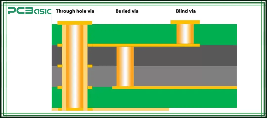
Although both back drilling and blind/buried vias can enhance signal integrity, there are obvious differences between them in terms of cost, process complexity and manufacturing.
|
Feature |
Back Drilling |
Blind/Buried Vias |
|
Manufacturing Cost |
Lower; adds one re-drill step |
Higher; needs sequential lamination |
|
Stub Removal |
Partial (stub ≤ 10 mil) |
Full elimination |
|
Process Complexity |
Single lamination + re-drill |
Multiple lamination cycles |
|
Signal Integrity |
Excellent for most high-speed nets |
Ideal but cost-intensive |
|
Design Flexibility |
Simple via design |
More restrictive stack-up |
|
Recommended For |
High-speed backplanes, 5G boards |
Ultra-dense HDI circuits |
In a nutshell, PCB back drilling has achieved approximately 90% improvement in signal performance at a lower cost. Therefore, it has become the preferred solution with better cost performance in high-frequency, high-layer-count designs.
In PCBasic, back drilling is not an additional service but a standard capability deeply integrated into the company's advanced PCB drilling and manufacturing processes. By integrating automated equipment with digital systems, PCBasic can stably and efficiently complete high-precision back drilling processes, ensuring signal integrity and traceability.
1. Precision Equipment
PCBasic has a fully automated factory. Its dedicated PCB drilling centers are equipped with multi-axis CNC machines, and the drilling depth control accuracy can reach ± 0.15mm, which can meet the precise processing requirements of high-layer and high-density PCBS.
2. Advanced Inspection & Control
Each circuit board undergoes strict depth control and quality monitoring during the back drilling process. X-Ray inspection is carried out to ensure the precise alignment of the drilling position with the inner copper foil, and cross-section analysis is conducted to verify that the residual stub has been completely removed without damaging the critical inner layer.
3. Engineering Integration
During the DFM stage, PCBasic’s engineering team will define and optimize the following parameters based on project requirements: layer pairings, oversize drilling, target residual stub length and minimum copper clearance.
Through the standardized definition of these parameters, we can ensure the repeatability and production consistency of each PCB back drilling.
4. Supported Applications
PCBasic’s back drilling technology is widely used in various high-frequency and high-speed electronic products, including 5G base stations and small cells, automotive radar modules, industrial IoT gateways, and servers and networking backplanes.
Back drilling provides a proven and cost-effective solution - it can remove those redundant copper segments like antennas, thereby ensuring impedance consistency and clean transmission of high-speed signals.
Through controlled depth precision, precise parameter setting and advanced inspection systems, PCB back drilling can transform ordinary multilayer circuit boards into reliable high-frequency interconnection structures.
For engineers who are designing the next generation of products, such as 5G infrastructure and automotive electronic devices, choosing a manufacturer like PCBasic that has mature back drilling capabilities means that every borehole can reach the highest standards in terms of depth, accuracy and signal integrity.
Back drilling is not merely a process in PCB drilling - it is a key bridge connecting high-speed design and dependable performance.

Assembly Enquiry
Instant Quote
Phone contact

+86-755-27218592
In addition, we've prepared a Help Center. We recommend checking it before reaching out, as your question and its answer may already be clearly explained there.
Wechat Support

In addition, we've prepared a Help Center. We recommend checking it before reaching out, as your question and its answer may already be clearly explained there.
WhatsApp Support

In addition, we've prepared a Help Center. We recommend checking it before reaching out, as your question and its answer may already be clearly explained there.