Global high-mix volume high-speed PCBA manufacturer
9:00 -18:00, Mon. - Fri. (GMT+8)
9:00 -12:00, Sat. (GMT+8)
(Except Chinese public holidays)
Global high-mix volume high-speed PCBA manufacturer
9:00 -18:00, Mon. - Fri. (GMT+8)
9:00 -12:00, Sat. (GMT+8)
(Except Chinese public holidays)
HomePage > Blog > Knowledge Base > Semi-Flex PCB Technology
Printed circuit boards are indispensable basic components in modern electronic products. In the past, engineers mainly used rigid PCBs to ensure structural strength and reliability, or chose flex PCBs made of polyimide to achieve bending and folding functions. However, both types have their drawbacks. A new solution that combines the advantages of both has emerged - the semi-flex PCB.
Semi-flex PCB is made of standard FR-4 material and thinned in specific areas of the circuit board through a precise depth-milling process, enabling these areas to bend moderately during installation. In this way, engineers can achieve localized flexible connections within a single board without the need for additional cables or connectors, thereby simplifying the assembly process, saving internal space, and enhancing overall reliability.
This article will introduce what a semi-flexible PCB is, its material composition, structural features, manufacturing process, key points of design and assembly, as well as the differences between semi-flexible PCBS and other types of boards.
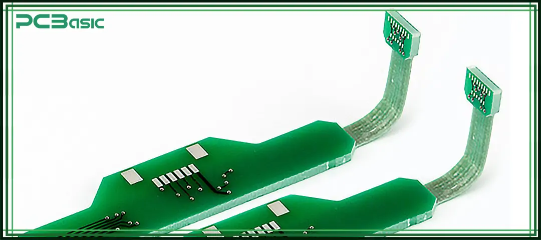
Semi-flex PCB (semi-flexible) is a special type of circuit board made using standard FR-4 material. It combines the strength of rigid PCBs and the bendability of flexible PCBs.
Unlike rigid circuit boards that cannot be bent at all or costly and fragile flexible circuit boards, semi-flex PCBs strike an ideal balance between the two - maintaining rigidity where stability is needed and providing flexibility where bending is required.
This type of PCB can achieve moderate bending of 30° to 180° by performing precise depth-milling in specific areas of the FR-4 substrate or by using a thin-core construction structure. It is specifically designed for static flexing or flex-to-install applications, that is, it is bent once during assembly and fixed into shape after installation, maintaining its shape throughout the entire service life.
This structure enables engineers to achieve flexible connections directly within one circuit board without the need for additional connectors or flat cables, thereby simplifying the assembly process, saving space and enhancing reliability.
More importantly, semi-flex PCBs can be produced on the same production line as standard rigid PCBs, without the need for additional molds or special equipment, significantly reducing manufacturing costs.
A semi-flex PCB is a type of circuit board made of specialized FR-4 epoxy glass laminate. This material is the same as the FR-4 used in standard rigid PCBs, but it has been improved to be more ductile and capable of achieving limited flexibility.
• Base Material: FR-4, with a glass transition temperature (Tg) range of 130–170 °C.
• Flexible Section Thickness: 0.10–0.30 mm after depth-milling.
• Copper Foil: 35 μm (1 oz), available as rolled annealed copper or electro-deposited copper.
• Layer Count: 2–8 layers, typically with 1–2 copper layers in the flexible area.
• Solder Mask: Flexible solder mask applied over the bend area; standard green solder mask on the rigid sections.
• Surface Finish: ENIG, OSP, Immersion Tin, or Immersion Silver.
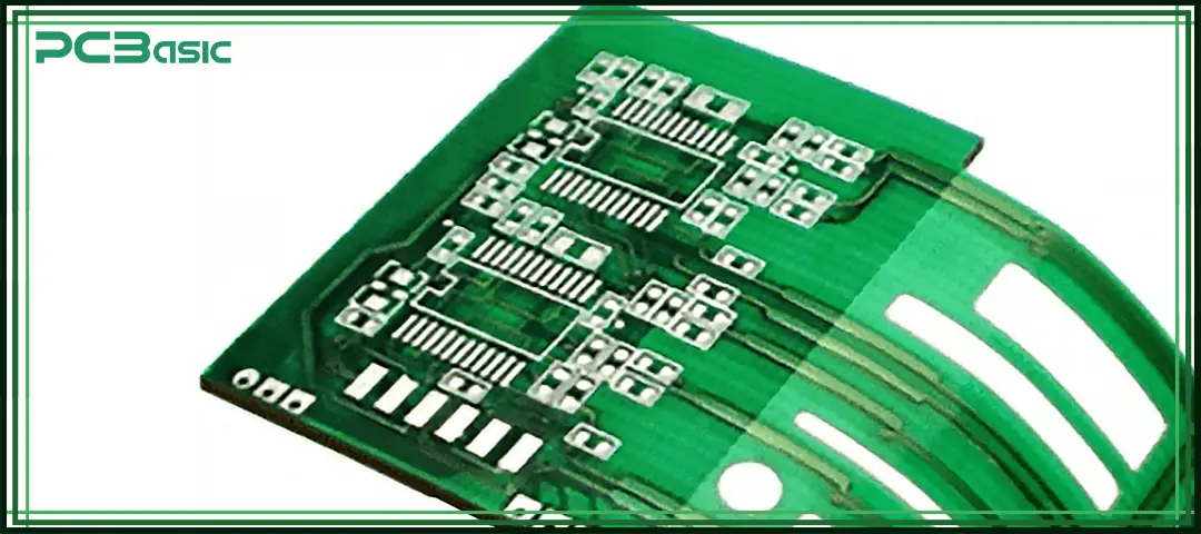
When designing semi-flex PCBs, we not only need to consider their electrical performance, but also their mechanical structure. Good design and installation methods can significantly enhance the service life and reliability of circuit boards. Now, here are some simple and practical design suggestions:
1. Bend Direction: When bending, make sure the copper foil is on the outside. This can prevent the copper layer from cracking or falling off during bending.
2. Keepouts: Do not place vias, pads or annular rings in the bend zone. It is best to maintain a safety distance of more than 1mm between the copper layer and the flexible zone to prevent stress damage.
3. Trace Spacing: In the bending area, the distance between the signal trace and the edge of the board should be no less than 0.3mm to avoid breakage or short circuit during bending.
4. Transition Radius: There should be a smooth radius at the junction of the rigid and the flexible area. It is recommended that the minimum radius be 1 mm, which can effectively disperse the bending stress.
5 Bending Radius: When bending, control the bending range, maintaining a minimum bending radius of 5mm and a maximum bending angle of 180° to ensure that the circuit board is not damaged after bending.
6. Panelization: It is recommended to manufacture semi-flex PCBs in panel form during production, as this makes operation easier and reduces the risk of damage during transportation and assembly.
7. Bending Process: During the bending process, warm air can be used to gently heat the flexible area, making the material easier to shape. The bending should be even and steady, and it is best to perform it on a fixed forming tool to avoid stress cracks.
As long as the above basic design and operation guidelines are followed, semi-flexible PCBs can maintain good dimensional stability and electrical integrity even after multiple assembly and bending. Ensure the long-term stable and reliable operation of the product.
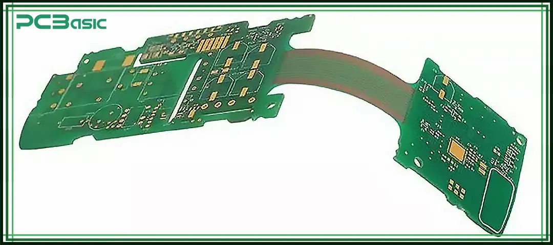
The production process of a semi-flexible PCB is very similar to that of a rigid PCB, and most of the steps are exactly the same. The only major difference is that a key step is added at the end - controlled depth milling or depth-milling of the flexible area. This processing technique precisely reduces the thickness of specific areas of the FR-4 material, thereby forming areas that can be bent.
Step-by-Step Process:
Select standard FR-4 laminate and clean and pre-treat the board surface to ensure there is no dust, oil or oxides.
Dry or wet film photoresist is applied, and the circuit pattern is formed through exposure and development. Then, etching is carried out to remove the excess copper layer, and the final circuit traces are made.
The multilayer semi-flex PCB is laminated under high temperature and pressure to firmly bond the copper foils, cores and prepregs together, forming a stable multilayer structure.
Drill through holes, tooling holes, and vias according to the design, and then perform through-hole plating to ensure electrical connectivity across layers. This step is exactly the same as the manufacturing process of a rigid PCB.
This is the core step of the entire semi-flex PCB. The thickness of FR-4 in the flexible area is precisely milled along the Z-axis using CNC equipment to be reduced to 0.1-0.3mm. This area will become thinner and lighter, thus having the ability to bend, but still safely support copper wiring.
According to the product requirements, surface finishes such as ENIG, OSP, Immersion Tin or Immersion Silver are carried out to ensure the reliability of soldering.
In the deep-milled flexible area, a flexible solder mask should be applied to prevent cracking during bending. Standard green solder mask is used in other areas.
Ensure that the circuit integrity, hole quality, thickness, and flex area precision of the semi-flex PCB are all qualified through methods such as AOI automatic optical inspection, flying probe testing, X-Ray or mechanical inspection.
Finally, the finished products are delivered in the form of assembled panels to avoid damage during transportation and assembly.
Time is money in your projects – and PCBasic gets it. PCBasic is a PCB assembly company that delivers fast, flawless results every time. Our comprehensive PCB assembly services include expert engineering support at every step, ensuring top quality in every board. As a leading PCB assembly manufacturer, we provide a one-stop solution that streamlines your supply chain. Partner with our advanced PCB prototype factory for quick turnarounds and superior results you can trust.
|
Technology Type |
Structure Description |
Manufacturing Method |
Advantages |
Ideal Applications |
|
Depth-Milled FR-4 Structure (SEMI.flex) |
Creates a flexible area on a standard FR-4 rigid board |
Performs depth-milling on the designated region |
• Simple process • Lower cost • Short production cycle |
Suitable for most flex-to-install applications |
|
Thin-Core Structure (BEND.flex) |
Uses a thin FR-4 core as the flexible area |
Does not rely on milling; bendability is created through the thin-core structure |
• More uniform flex-area thickness • More stable structure • Better for strict mechanical requirements • No polyimide required, still cheaper than rigid-flex PCB |
Suitable for designs requiring higher structural stability and tight dimensional control |
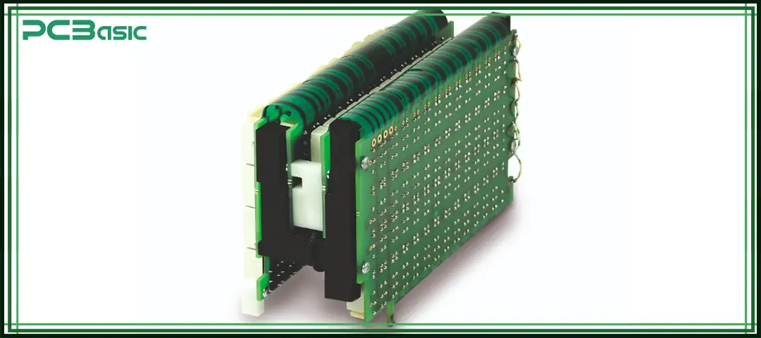
|
Characteristic |
Typical Specification |
|
Material |
FR-4, Tg 130–170 °C |
|
Flexible Section Thickness |
0.10–0.30 mm |
|
Copper Weight |
35 μm |
|
Bend Radius |
≥ 5 mm |
|
Max Bend Angle |
90°–180° |
|
Max Number of Bends |
5 (static) |
|
Layer Count |
2–8 layers |
|
Track/Gap |
0.075 / 0.075 mm |
|
Surface Finish |
ENIG, Immersion Tin/Silver, OSP |
|
Typical Board Size |
Up to 538 × 610 mm |
|
Applications |
Automotive, Industrial, Medical, Consumer Electronics |
To understand where the semi-flex PCB fits in the PCB ecosystem, it’s useful to compare it with other types.
|
Feature |
Rigid PCB |
Flex PCB |
Rigid-Flex PCB |
Semi-Flex PCB |
|
Flexibility |
None |
Full |
Partial (flex + rigid zones) |
Localized (FR-4 bend area) |
|
Material |
FR-4 |
Polyimide |
FR-4 + Polyimide |
FR-4 (thinned) |
|
Bending Cycles |
0 |
Infinite |
Infinite |
≤ 5 (static) |
|
Application Type |
Fixed boards |
Dynamic motion |
Dynamic + structure |
Static (flex-to-install) |
|
Manufacturing Complexity |
Simple |
Complex |
Very complex |
Moderate |
|
Cost |
Low |
High |
Very high |
Low to medium |
|
Assembly |
Easy |
Special handling |
Moderate |
Easy (standard SMT) |
|
Layer Count |
Up to 30 |
Up to 6 |
Up to 10 |
2–8 |
|
Typical Use |
General electronics |
Wearables, FPCs |
Aerospace, high-end |
Automotive, industrial, IoT |
Therefore, the semi-flex PCB lies precisely in between - cheaper and easier to produce than rigid-flex boards, and more flexible than traditional rigid boards. Semi-flex PCBs are highly suitable for electronic products that only require limited bending, high reliability, and extreme space utilization, making them an ideal choice that balances cost and performance.
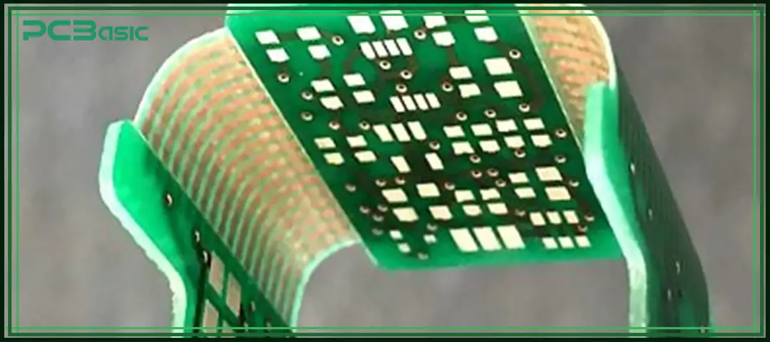
Semi-flex PCBs have been widely used in multiple industries due to their flexibility, reliability and cost advantages. Typical applications include:
Automotive Electronics
Used in lighting systems, sensors, EV battery modules, and infotainment systems.
The semi-flex PCB withstands vibrations while allowing compact installation within tight enclosures.
Industrial Automation
Found in robotics, control units, actuators, and measurement devices.
Flexible zones absorb mechanical stress, improving product longevity.
Medical Equipment
Ideal for wearable monitors, imaging systems, and portable diagnostic tools where both flexibility and stability are critical.
Consumer Electronics
Common in smartphones, laptops, LED modules, and compact IoT devices.
Enables 3D assembly and thin product profiles.
Aerospace and Defense
Suitable for navigation systems, avionics, and space modules where vibration resistance and reliability are key.
In all the above-mentioned industries, semi-flex PCB technology offers significant advantages such as low-cost flexibility, reduced wiring, and simplified assembly, which are highly in line with the development trend of miniaturization and lightweighting of modern electronic products.
With the continuous development of electronic products towards smaller size, lighter weight and higher integration, semi-flex PCBs are gradually becoming an excellent solution that is practical and can be mass-produced on a large scale.
The semi-flex PCB combines the mechanical strength of the rigid PCB with the localized bendability of the flex circuit, achieving an ideal balance among reliability, cost-effectiveness and manufacturability. It not only reduces connectors and lowers assembly complexity, but also enables a compact 3D structure configuration. Meanwhile, it is still produced based on the standard FR-4 process, featuring high compatibility and cost-effectiveness.
Whether in automotive systems, medical devices, industrial control or consumer electronics, semi-flex PCBs are changing the way engineers deal with the design of confined spaces. With the continuous improvement of material performance and the steady advancement of manufacturing technology, semi-flexible circuit boards with higher layer counts, finer line widths/spacings, and more 3D interconnection innovations will emerge in the future.
For any electronic product designer who needs to be both flexible and cost-controllable, the semi-flex PCB is not a compromise solution but a new standard for efficient and reliable electronic manufacturing in the new era.
Assembly Enquiry
Instant Quote
Phone contact

+86-755-27218592
In addition, we've prepared a Help Center. We recommend checking it before reaching out, as your question and its answer may already be clearly explained there.
Wechat Support

In addition, we've prepared a Help Center. We recommend checking it before reaching out, as your question and its answer may already be clearly explained there.
WhatsApp Support

In addition, we've prepared a Help Center. We recommend checking it before reaching out, as your question and its answer may already be clearly explained there.