Global high-mix volume high-speed PCBA manufacturer
9:00 -18:00, Mon. - Fri. (GMT+8)
9:00 -12:00, Sat. (GMT+8)
(Except Chinese public holidays)
Global high-mix volume high-speed PCBA manufacturer
9:00 -18:00, Mon. - Fri. (GMT+8)
9:00 -12:00, Sat. (GMT+8)
(Except Chinese public holidays)
HomePage > Blog > Knowledge Base > The Ultimate Guide to PCB Routing
PCB routing is not merely about drawing a few copper lines; it is a crucial step in truly transforming a circuit schematic into a functional circuit board. Proper circuit routing is not only about connectivity; it also involves ensuring signal integrity, reducing crosstalk, managing heat dissipation, and meeting manufacturing requirements. Unreasonable routing can lead to reflections, EMI issues and even rework, while following PCB routing best practices and PCB routing guidelines can ensure a stable and reliable design.
Modern design tools offer automation features such as AI PCB Design and AI PCB layout, which can help quickly complete partial electrical routing and optimization.
This guide will combine the proven routing guidelines for PCBs, practical PCB layout tips, and the increasingly important AI circuit board tools. From component placement to final verification, it helps both beginners and experienced designers complete efficient, reliable and scalable AI circuit board design.
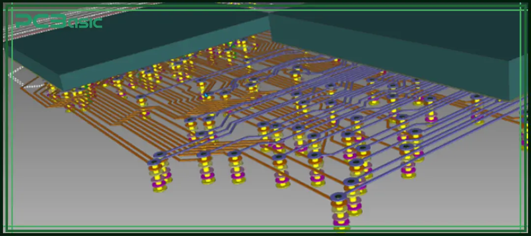
PCB routing is the process of defining copper traces on a printed circuit board to connect electronic components. Each PCB line transmits signals, power and ground between components according to the circuit schematic. In simple terms, PCB routing is the process of turning a circuit diagram into a physical circuit board that can be manufactured.
Wire routing determines the flow path of current on the circuit board. Correct circuit routing is not merely about connecting wires; it requires ensuring signal integrity, reducing crosstalk, improving heat dissipation, and avoiding electromagnetic interference (EMI). If the wiring is not reasonable, it may cause reflection, timing errors, and even lead to rework. Following the PCB routing guidelines and PCB routing best practices can ensure the stability and reliability of the circuit board.
Modern design software, such as AI PCB Design and AI PCB layout, can automatically complete some electrical routing, such as routing planning, impedance control and length matching. These tools are very useful in the design of high-density AI circuit boards. However, for key issues such as differential pair routing, via selection, and impedance control, the judgment and experience of engineers are still required.
Nowadays, many modern design software (such as Altium Designer, Cadence Allegro, KiCad, Mentor Xpedition, etc.) have ready integrated AI-assisted functions, which can provide intelligent suggestions in PCB design and layout, such as routing planning, impedance control and length matching. These tools have significant advantages in the design of high-density circuit boards. However, for key links such as differential pair routing, via selection and complex impedance control, experienced engineers are still needed to make judgments and optimizations.
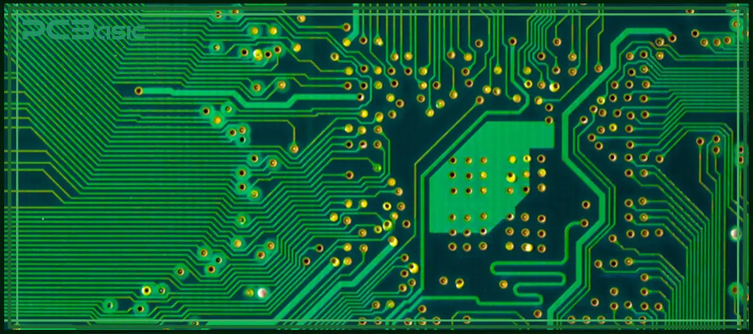
When designing PCBs, many challenges that affect the quality of the final product will be encountered. Understanding these issues helps us better apply the PCB routing guidelines to avoid common pitfalls.
|
Challenge |
Description |
Solution |
|
Component Density |
High-density boards with many components make routing complex, increasing the risk of crosstalk and signal integrity issues. |
Use AI PCB layout tools to assist with partitioning and layer assignments; apply PCB layout tips to pre-plan routing directions. |
|
High-Speed Signal Routing |
High-frequency signals can cause reflections, impedance mismatches, and EMI. |
Apply PCB routing techniques such as differential pair routing and controlled impedance traces, ensuring length matching. |
|
Design Rule Complexity |
Different nets may require distinct widths, clearances, or layer assignments. Ignoring these rules may lead to failures or manufacturability issues. |
Follow structured routing guidelines for PCB, and assign specific design rules for critical signals. |
|
Thermal and Power Management |
High-current traces and power planes, if poorly routed, may lead to overheating or system failure. |
Follow PCB routing best practices by widening power/ground traces, using multiple power/ground planes, and adding thermal vias. |
|
Manufacturing Constraints |
Fabrication limits impose restrictions on trace width, spacing, via sizes, and copper pours. |
Confirm manufacturer capabilities early in design; use PCB routing techniques that account for manufacturability to reduce errors and costs. |
The right tools can significantly improve PCB routing techniques.
Popular tools for PCB routing:
• PCB editors: Altium Designer, KiCad, Cadence Allegro, etc.
• Autorouters: Handle simple connections but require cleanup.
• Interactive routing tools: Slide routing, fanout routing, differential pair routing.
• Constraint managers: Enforce length matching, spacing, and impedance rules.
• Signal integrity and DFM tools: Simulate and analyze electrical and manufacturing performance.
By using these tools and combining them with PCB routing best practices, we can enhance efficiency and minimize errors in both manual and AI circuit board design workflows.
Adhering to PCB routing guidelines ensures robust and manufacturable designs.
• Separate analog and digital signals to reduce interference.
• Avoid 90° trace bends; use smooth curves.
• Maintain consistent trace widths and spacing for impedance control.
• Use ground and power planes strategically.
• Route critical nets first, followed by less sensitive connections.
• Place decoupling capacitors close to power pins.
• Alternate trace directions on adjacent layers to reduce crosstalk.
• Minimize via usage and optimize their placement.
By following these PCB routing techniques, efficient wire routing can be achieved, and the reliability of the entire PCB can be enhanced.
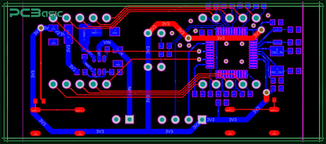
A structured PCB routing workflow can enhance efficiency, reduce errors, and ensure that the design adheres to the PCB routing guidelines. The typical process usually includes: component layout, signal routing, power and ground routing, differential pair routing, via arrangement and final verification.
A reasonable component placement is the first step in PCB routing. A good placement can shorten the trace length, reduce noise and simplify wire routing.
Although design software can optimize the placement, ultimately, manual checks are still required to comply with PCB routing best practices.
After completing the component placement, traces need to be established between pins. The routing must follow the PCB routing guidelines to ensure signal integrity.
The routing of the power supply and ground directly affects the stability of the circuit. Using a complete power/ground plane can reduce voltage drop and EMI.
PCB routing best practices:
• Keep power and ground traces wide enough to carry the required current.
• Place ground planes beneath sensitive signals to minimize impedance.
• Position decoupling capacitors close to power pins.
• Avoid unnecessary splits in ground planes to maintain a stable reference voltage.
Time is money in your projects – and PCBasic gets it. PCBasic is a PCB assembly company that delivers fast, flawless results every time. Our comprehensive PCB assembly services include expert engineering support at every step, ensuring top quality in every board. As a leading PCB assembly manufacturer, we provide a one-stop solution that streamlines your supply chain. Partner with our advanced PCB prototype factory for quick turnarounds and superior results you can trust.
High-speed signals require differential pair routing to maintain signal integrity.
PCB routing techniques:
• Precisely match trace lengths.
• Keep uniform spacing to ensure controlled impedance.
• Insert ground vias between pairs for low-impedance return paths.
• Avoid crossing high-speed signals at right angles.
Vias are used for interlayer connections. A reasonable arrangement can improve signal quality and heat dissipation performance.
After the wiring is completed, verification must be carried out to ensure compliance with the PCB routing guidelines for PCB and satisfaction of manufacturing requirements.
Adhering to PCB routing guidelines ensures robust and manufacturable designs.
Top PCB routing best practices:
• Separate analog and digital signals to reduce interference.
• Avoid 90° trace bends; use smooth curves.
• Maintain consistent trace widths and spacing for impedance control.
• Use ground and power planes strategically.
• Route critical nets first, followed by less sensitive connections.
• Place decoupling capacitors close to power pins.
• Alternate trace directions on adjacent layers to reduce crosstalk.
• Minimize via usage and optimize their placement.
Complex PCBs often require advanced PCB routing techniques:
• Differential pair routing for high-speed signals.
• Impedance-controlled traces for signal integrity.
• Serpentine trace tuning for length matching.
• Hierarchical and bus routing for organized, efficient layouts.
• Thermal vias and pads for improved heat dissipation.
Mastering PCB routing is the key to designing high-performance, reliable and manufacturable circuit boards. Whether it is wiring routing or high-speed differential pair routing, each PCB line will directly affect the function of the circuit and the integrity of the signal.
By making reasonable use of AI PCB design tools and mastering practical PCB layout tips, designers can complete the optimized wiring more efficiently. Meet the demands of modern electronic products. Follow mature PCB routing techniques and strictly implement routing guidelines for a PCB, and adhering to the PCB routing best practices can ensure that the electrical routing is clear, efficient and stable.
Whether you are a beginner or an experienced designer, as long as you understand what PCB routing is and apply these principles in actual design, you can improve the quality of circuit board design, reduce rework, and make product performance more reliable.
Assembly Enquiry
Instant Quote
Phone contact

+86-755-27218592
In addition, we've prepared a Help Center. We recommend checking it before reaching out, as your question and its answer may already be clearly explained there.
Wechat Support

In addition, we've prepared a Help Center. We recommend checking it before reaching out, as your question and its answer may already be clearly explained there.
WhatsApp Support

In addition, we've prepared a Help Center. We recommend checking it before reaching out, as your question and its answer may already be clearly explained there.