Global high-mix volume high-speed PCBA manufacturer
9:00 -18:00, Mon. - Fri. (GMT+8)
9:00 -12:00, Sat. (GMT+8)
(Except Chinese public holidays)
Global high-mix volume high-speed PCBA manufacturer
9:00 -18:00, Mon. - Fri. (GMT+8)
9:00 -12:00, Sat. (GMT+8)
(Except Chinese public holidays)
HomePage > Blog > Knowledge Base > An Ultimate Guide on PCB Assembly Drawing
The PCB assembly drawing is a small part of the overall PCB assembly process. It is one of the most important tools that will assist you in flawless fabrication and assembly. A PCB drawing usually has component placement information, multi-layer diagrams, assembly notes, etc. So, it helps in reducing manufacturing errors, compliance errors and misinterpretation. Also, this assembly drawing guarantee your design to be built properly and working as needed.
In this comprehensive blog, we will cover everything you need to know to master PCB assembly drawing. Additionally, mastering PCB assembly drawings will help you avoid costly mistakes and production delays.

The PCB assembly drawing is going to give you a detailed visual and written instructions on how to assemble electronic components or parts on PCBs. The basic purpose of this fabrication drawing is to convey the design intent into the assembly team. That’s how it reduces mistakes. Furthermore, it will ensure that the product fulfills the expected standards.
This PCB drawing is designed by engineers who are very skilled and have a lot of experience. Also, this drawing helps OEMs to ensure that the products are manufactured as per the specs defined.
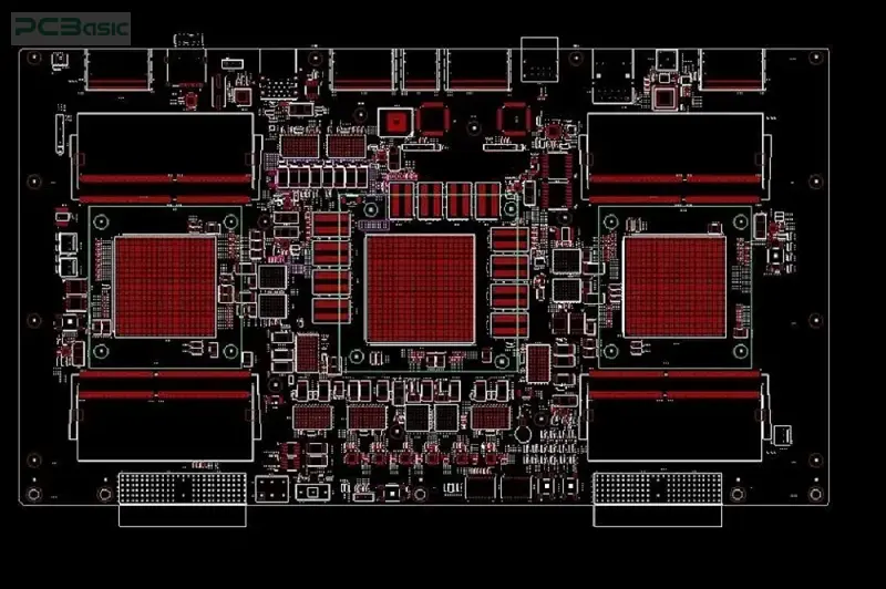
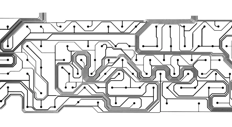
This assembly drawing includes important information like polarity of components, location of each component on the board, routing of traces, and reference designators for identification. It may also include orientation of parts, special assembly instructions, and placement of vias and holes.
PCB assembly drawing serves multiple crucial purposes. Some of these are mentioned below.
1. Ensures Design Intent
The PCB drawing visually shows your design intent. It also ensures that the PCB is assembled according to your specifications and requirements. As a result, this drawing prevents performance problems and functionality issues.
2. Streamline Production Workflow
Assembly drawing provides all assembly details in one place. So, assemblers don’t waste their time figuring out unclear areas. Hence, it increases the production rate and can also reduce costs.
3. Support Quality Control
The drawing helps to meet quality standards. This document makes easy to inspect PCBs and identify any production errors. Therefore, these drawings are important for error free manufacturing. In addition, they ensure your design works exactly as intended.

Understanding the key elements of PCB fab drawing is crucial for manufacturers, engineers, and technicians. This understanding ensures the efficient and error-free production of electronic devices. A PCB assembly drawing example demonstrates how a PCB fab drawing can increase the production process. Here are the key elements of the PCB assembly drawing:
The board outline and dimensions illustrates the shape and size of the PCB. This section provides the length, width, and other critical dimensions of the board. Additionally, it contains reference dimensions to help in proper component placement. This section also outlines the exact shape of the PCB, including any notches or cutouts.
Furthermore, the board outline and dimensions may show locations of cutouts for displays and connectors. It can also depict the positions of mechanical PCB features or any slots.
The component placement and orientation indicate the exact location of components on the board. This section, often, include the assembly order number next to the parts. That's how it indicates the sequence. It also shows the location of crucial components first. In this way it sets position reference for other parts.
This section can also depicts orientation of components and can group parts into functional sections for easy assembly. Additionally, it uses arcs, lines, or other indications to specify the orientation of polarize components. Hence, this element can accurately reflect the PCB layout.
The bill of materials is a list of all the components required for the assembly. This list includes supplier info, part numbers and their quantities. BOM make sure that the assembly team has all required components. Furthermore, it ensures that the team can do replacements if needed. This element also helps in cross referencing components with their respective reference designators. That way, BOM facilitate error-free assembly process.
Assembly notes include specific manufacturing instructions that cannot be easily communicated through diagrams alone. A few of these guidelines are specifications, special feature locations, assembly details, and specific requirements for testing and inspection.
In addition, these notes include a list of parts. However, it is only available when manufacturers request it. By including these details, this element ensures that the fab assembly process meets the quality standards.
PCB assembly drawing often use visual enhancements like symbols and annotations to give additional information. For example, fiducial markers are used for automated assembly machines. Similarly, polarity markers shows the correct orientation for polarized parts like electrolytic capacitors and diodes. These visual enhancement guides the assembly team and prevent common assembly errors.
All these elements can be modified or added to suit any specific requirements of a client. More than this, you can even omit any of these elements if it does not apply to your client’s assembly drawing. However, you should consult your contract manufacturer when choosing the right elements to use in your drawing. He will tell you what he requires to generate your PCB. In this way, you can avoid repeating an entire PCB assembly drawing.
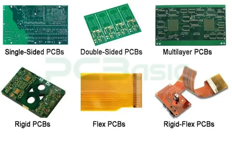
Understanding the different types of drawings for various PCB needs is crucial to meet high level functionality. Here are the major types of drawings for various PCB needs.

A single-sided PCB is the most common type of PCB. It has a single copper layer above the substrate. Due to one conducting layer, the conductive paths can't overlap and hence take up a lot of space. These boards are used for low-cost and basic electronic instruments. These tools include power suppliers, FM radios, calculators, timing circuits, LED lighting boards, etc.
In double sided boards, a thin layer of conducting material is added on both sides of the board. The PCBs connect the circuits on either side through surface mount technology or hole technology. These boards are used in power monitoring, test equipment, cell phone systems, HVAC applications, UPS systems, amplifiers, and so on.
You can fold or twist a flex PCB. It is made up of many circuits and parts. These parts are arranged on a flexible substrate. Flex PCB is usually made from transparent conductive polyester film, polyamide, or a polyether ether ketone (PEEK). These PCBs are available in single-sided, double-sided, or multi-layer configurations. Flex PCBs are used in automotive industries, laptop computers, cellular telephones, OLED fabrication, flex solar cells, and LCD fabrication.
A Rigid-Flex PCB is a hybrid circuit board. It includes characteristics from both flexible and rigid circuit boards. Such designs are complex in nature since the construction of such boards is 3D. These boards have the light weight advantage. So, they suit for a wide range of applications such as aerospace and medical field.
Specialized assemblies are developed to meet unique industry requirements. Therefore, these will help to prevent errors and comply with specific industry regulations. Through customized assembly drawings, manufacturers can create detailed drawings to enhance functionality.
PCB fab drawing serves as a link between the manufacturing stages and final product. This fabrication drawing makes sure that the designer's intent is perfectly shown in functional product. Some other benefits of PCB fab drawing are:
Assembly drawing ensures accuracy in the assembly process. It provides a detailed view of the PCB. This view includes the orientation of each component and its position. This drawing also gives exact specifications and measures.
PCB fabrication drawing is one of the most important quality control tools. The inspection team compares this drawing to the actual assembled boards to ensure they meet the specified design criteria. By this comparison, inspectors can easily identify any defects or errors. Hence, this step will keep the quality at the next level. Furthermore, it ensures that only fully functional products reach the market.
Assembly technicians, designers, and engineers all use these drawings to convey their expectations and requirements. This common reference point ensures that everyone is on the same page. In addition, it will help to minimize misunderstandings. As a result, the manufacturing process becomes more efficient, which will reduce errors and delays.
In conclusion, the above-mentioned elements of the PCB assembly drawing can help in materializing error-free PCB design. This would also help to successfully achieve the expectations and demands of the client. However, any mistake in PCB drawing may raise the entire cost of production in addition to a delay. So, it makes sense to reach out to a trusted and reputed assembly service provider.
Hence, if you are looking for such an assembly service provider then PCBasic really stand out of the crowd. You can hire our PCB manufacturing and assembly drawing with a professionally qualified team with many years of experience. Our professionals PCB assembly drawing services successfully help your business in adopting the cutting-edge technologies.

Assembly Enquiry
Instant Quote
Phone contact

+86-755-27218592
In addition, we've prepared a Help Center. We recommend checking it before reaching out, as your question and its answer may already be clearly explained there.
Wechat Support

In addition, we've prepared a Help Center. We recommend checking it before reaching out, as your question and its answer may already be clearly explained there.
WhatsApp Support

In addition, we've prepared a Help Center. We recommend checking it before reaching out, as your question and its answer may already be clearly explained there.