Global high-mix volume high-speed PCBA manufacturer
9:00 -18:00, Mon. - Fri. (GMT+8)
9:00 -12:00, Sat. (GMT+8)
(Except Chinese public holidays)
Global high-mix volume high-speed PCBA manufacturer
9:00 -18:00, Mon. - Fri. (GMT+8)
9:00 -12:00, Sat. (GMT+8)
(Except Chinese public holidays)
HomePage > Blog > Knowledge Base > NPN and PNP Transistors: A Comprehensive Guide
Transistors play roles such as switching, amplification, signal processing and power control in circuits. There are many types of transistors. Among them, NPN transistors and PNP transistors are the most widely used. Both belong to BJT (Bipolar Junction Transistor). There are differences between NPN and PNP, and they cannot be interchanged. It is important to understand the structure, symbol, working mode and differences between the two.
Next, this article will explain them from aspects such as working principles, symbols, and applications. Before elaborating on these two types of transistors, let's have a general understanding of transistors first.
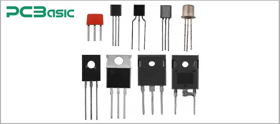
Transistors are one of the core and fundamental components in modern electronic devices. They can perform functions such as logic control, power drive, and signal processing. Transistors can be found in micro-sensors, household electronic products, and complex industrial systems.
A transistor is a device made of semiconductor materials that can switch, amplify or regulate electronic signals by controlling current or voltage. It consists of three layers of semiconductor materials that have been "doped". The doped materials exhibit two types of characteristics:
N-type: contains extra electrons
P-type: has "holes", which are positions where electrons are missing.
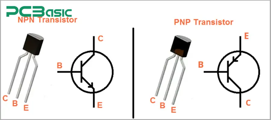
One of the most common structures of transistors is the bipolar junction transistor (BJT). A BJT is composed of two types of semiconductor materials alternately. A typical BJT transistor consists of three electrodes:
Base: Control terminal for the transistor
Collector: Terminal where the conventional current enters
Emitter: Terminal where the conventional current exits
In actual circuits, transistors typically have three common operating modes:
Cutoff: It is equivalent to an open circuit, with almost no current flowing through the C–E junction.
Amplification: It can linearly amplify signals.
Saturation: It is equivalent to a closed switch, with the current between the C–E junction fully conducting.
Transistors can play multiple roles in electronic systems. There are also various types of transistors. Below, we will introduce the main types of transistors to you.
Depending on the different conductive mechanisms, structures and application fields, transistors can be classified into the following major types:
|
Category |
Description |
Typical Applications |
|
BJT (Bipolar Junction Transistor) |
Formed by alternating N-type and P-type semiconductor layers; current-controlled device. Includes NPN and PNP structures. |
Amplifiers, switching circuits, signal processing |
|
MOSFET (Metal-Oxide-Semiconductor FET) |
Voltage-controlled device with very high input impedance; available in N-channel and P-channel types. |
Power management, switching power supplies, microcontroller interfaces |
|
JFET (Junction FET) |
Voltage-controlled conduction channel; simple structure and low noise. |
Analog amplification, input stages |
|
IGBT (Insulated Gate Bipolar Transistor) |
Combines MOSFET input characteristics with BJT conduction capability; suitable for high power. |
Motor drives, inverters, EV power systems |
|
Darlington Transistor Pair |
Two BJTs connected together to provide very high current gain. |
Motor control, high-current switching |
|
Phototransistor |
Light-sensitive transistor that modulates current based on light intensity. |
Light sensors, optical switching |
|
UJT (Unijunction Transistor) |
Single-junction device used mainly for triggering and timing. |
Oscillators, waveform generators, triggering circuits |
Alright, after having a general understanding of the relevant content about transistors, next, we will introduce the NPN and PNP transistors separately.
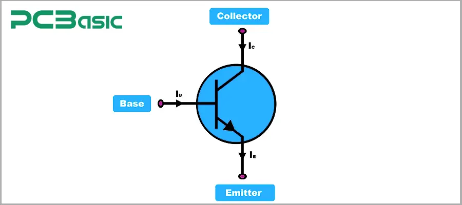
The NPN transistor is one of the two basic structures of bipolar transistors (BJTs). Just as its name suggests, it is composed of a layer of P-type semiconductor sandwiched between two layers of N-type materials. This arrangement determines the current path of the device and the way it responds to the input signal.
Inside an NPN transistor, these three layers of semiconductor materials correspond to the emitter, the base, and the collector. The emitter is heavily doped to provide a large number of electrons; the base is lightly doped to allow most of the electrons to pass through smoothly; and the collector is used to absorb and collect these charge carriers. This structural design enables the transistor to regulate a larger current from the collector to the emitter through a small current at the base. Now, let's look at the working principle of an NPN transistor.
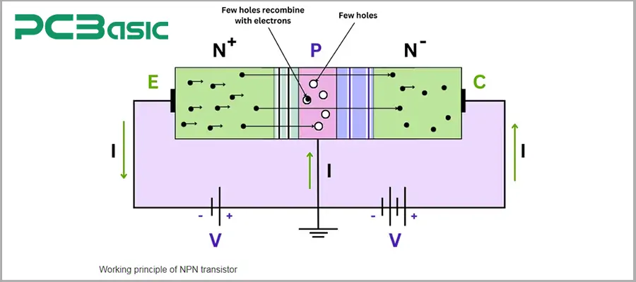
The working principle of an NPN transistor is to control the larger current between the collector and the emitter through a small current at the base. When a small forward voltage is applied to the base-emitter junction, the junction is forward-biased, and electrons will be injected from the emitter to the base. Then, due to the very thin and low-doped nature of the base region, only a small number of electrons will combine with the holes in the base, while most electrons will continue to move forward and flow towards the reverse-biased base-collector junction. The reverse bias forms an electric field on this junction, pulling the electrons from the base "to" the collector, thereby creating a larger current between the collector and the emitter. This is the working principle of an NPN transistor. This working process can be simply understood as:
Adding a little positive voltage to the base
→ The electrons in the emitter will be "fed" into the base.
The base is very thin
→ Most of the electrons will not stay but pass through quickly.
There is a reverse bias between the base and the collector
→ There is an electric field there that will "pull" the electrons to the collector.
Result: A small base current controls a much larger collector current.
Understanding the current flow mechanism of NPN also helps to distinguish the differences between NPN and PNP.
The NPN transistor plays a central role in modern electronic design. It is crucial to understand its application in actual circuits. Its usage is extensive, and the following will introduce some of the main application types:
1. Digital switches and logic control
One of the most basic applications of the NPN transistor is the low-side digital switch. This can be achieved with a very small base current, which enables the transistor to conduct, thereby allowing a larger collector-emitter current to pass through. NPN devices are commonly used in the following applications in this field:
Output switch for microcontrollers (MCU)
LED driver
Logic level conversion
Signal inversion
Relay and solenoid valve drive
2. Analog Signal Amplification
The electrons in an NPN transistor can easily pass through the very thin base region, which makes it widely used in the field of analog amplification. When in the amplification region, a weak input signal can be amplified into a larger output signal. Typical applications include:
Audio preamplifier and gain stage
Instrument amplification circuit
Radio frequency amplifier
Sensor signal conditioning
Mixing and oscillator circuit
3. Motors, relays and high-current load driving
Another important application of NPN devices is to drive inductive or high-current loads. As a low-end driver, the NPN transistor can control the following loads:
DC motor
Relay coil
Electromagnetic valve
Buzzer or vibrator
High-power LED or light strip
4. High-speed Switches in Power Electronics
Although modern power supplies mostly use MOSFETs, high-speed NPN BJTs are still widely used in:
Switching power supplies
Inverter circuits
Drive stages of MOSFETs and IGBTs
PWM control circuits
High-frequency oscillation modules
5. Sensor interface and logic level detection
NPN transistors are commonly used to convert weak or analog sensor signals into clean logical outputs. Typical applications include:
Infrared receiving module
Photoresistive circuit
Hall magnetic sensor
Gas and temperature sensor interface
Threshold detection circuit
6. Digital Output Protection and Isolation
The NPN transistor can also be used for interface protection and current buffering. In many transistor diagrams, you will see the NPN stage located between the weak logic output and the high current load, serving to:
Provide current amplification
Prevent reverse current
Isolate sensitive IC pins
Perform level conversion between 3.3V and 12V systems
7. NPN–PNP Complementary Circuit
In more complex circuits, NPN and PNP transistors are combined to form a complementary structure, for example:
Push-pull output stage
AB-type amplifier
Complementary Darlington pair
Buffer and inverter
Symmetrical analog stage
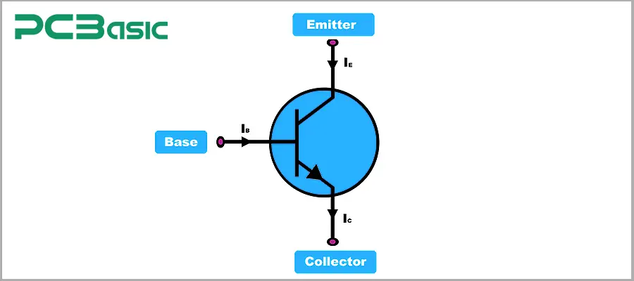
The PNP transistor is another basic structure of the bipolar transistor (BJT). The PNP transistor is the complementary structure of the NPN transistor, and its P–N–P hierarchical structure determines the direction of carrier movement. When viewing the customers’ transistor diagram or transistor symbol, it is necessary to first confirm whether the circuit uses NPN or PNP, as the difference between NPN and PNP will directly affect polarity, current path, and the soldering direction of the component on the PCB.
Unlike the NPN transistor which uses electrons as the main carrier, the PNP uses holes as the main carrier. The arrow in the PNP transistor symbol points towards the base, opposite to the outward arrow in the NPN transistor symbol. Be sure to carefully review if there is a PNP transistor direction in the design, as incorrect symbol, pin, or package direction annotations will lead to failure of power-on on the circuit.
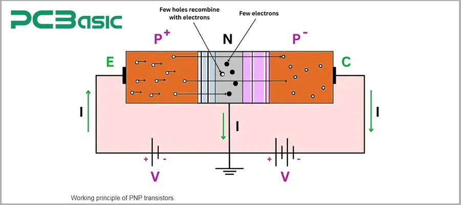
The PNP transistor operates by allowing holes to flow from the emitter to the collector, with the flow controlled by a very small base current. It has a similar control mechanism to the NPN transistor, but the polarity is completely opposite.
When the base-emitter junction is forward-biased when the base voltage is slightly lower than the emitter (about 0.6–0.7V), holes from the P-type emitter enter the lightly doped N-type base region. Due to the thinness of the base region, most of the holes do not recombine but continue to move towards the reverse-biased collector. The electric field at the collector attracts these holes, allowing a very small base current to control a much larger emitter-collector current.
During the PCB assembly and testing process in PCBasic, engineers will confirm whether the PNP components are operating within the correct working range:
Active Working Area
Emitter–Base junction forward biased, Base–Collector junction reverse biased. PCBasic uses AOI to verify transistor orientation and soldering quality, while ICT/FCT is used to confirm whether the electrical parameters—such as gain and bias—are within the normal operating range.
Cutoff Area
Both junctions are reverse biased, no current flows.
Saturation Area
Both junctions are forward biased, the transistor is fully conducting. In many customers’ power boards and control boards, PNP is used as a high-side switch. PCBasic will provide appropriate heat dissipation and copper spreading design suggestions for these devices.
Understanding these principles helps to avoid assembly errors and ensures that the PCBA can function as designed.
In fact, in PCB manufacturing, the co-occurrence of PNP transistors and NPN transistors is very common. We have previously introduced the application of NPN transistors. Now, we will introduce the common applications of PNP transistors.
1. High-side switch in power control
In the high-side drive circuit, PNP transistors are used, connecting the load on the positive power side and having the PNP transistor supply the current. This characteristic of the PNP transistor is very intuitive. Common applications include:
Automobile control module
Intelligent battery system
Industrial control cabinet
Sensor distribution board
Power bypass and switch circuit
2. Complementary Push-Pull Output Stage
PNP and NPN are often used together in push-pull amplification circuits. Common devices include:
Audio power amplifier
Control system amplification module
Precision measuring instrument
High linearity analog drive
3. Linear Voltage Regulation and Voltage Adjustment
PNP transistors are used as the high-side adjustment component in many linear voltage regulators to maintain a stable output voltage. Common examples include:
Low-noise sensor power supply
Analog reference power supply
Medical electronic control circuit
Voltage regulator interface for converting 24V to 5V in the industry
4. Current Mirror and Bias Circuit
In high-precision analog circuits, PNP is an important component for forming a current mirror and is often used in conjunction with NPN. Common application scenarios include:
Differential amplification bias
Precise reference current source
Temperature compensation circuit
Analog front-end circuit
5. Industrial sensor output (source-type output)
Many industrial sensors use PNP as the "source-type output". When the sensor is triggered, the output terminal will be raised.
6. Integrating Logic and Power Management Circuits
In complex circuits, PNP is used to handle:
Power-on sequence
Load switching
Soft start
Reverse connection protection
Low-power standby switching
Here are the differences between NPN and PNP transistors.
|
Comparison Item |
NPN Transistor |
PNP Transistor |
|
1. Semiconductor Structure |
N-type – P-type – N-type |
P-type – N-type – P-type |
|
2. Majority Carrier Type |
Electrons (faster) |
Holes (slower) |
|
3. Basic Working Principle |
Electrons flow from emitter to collector; the base controls electron injection |
Holes flow from emitter to collector; the base controls hole injection |
|
4. Conventional Current Direction (transistor diagram) |
Current flows from collector to emitter |
Current flows from emitter to collector |
|
5. Biasing Method |
BE junction must be forward-biased (base more positive than emitter) |
BE junction must be forward-biased (base more negative than emitter) |
|
6. Switching Condition |
Turns on when the base is driven positive |
Turns on when the base is driven negative |
|
7. Transistor Symbol |
NPN symbol: arrow points outward (electrons emitted outward) |
PNP symbol: arrow points inward (holes flowing inward) |
|
8. How to Identify the Symbol |
Arrow Not Pointing in (points outward) → NPN |
Arrow Pointing in (points inward) → PNP |
|
9. Control Mode Difference (npn vs pnp transistor) |
Low-side switching; load connected to VCC and NPN connects to ground |
High-side switching; load connected to ground and PNP connects to VCC |
|
10. Input Drive Method |
MCU outputs HIGH → NPN turns on |
MCU outputs LOW → PNP turns on |
|
11. Advantages |
Faster, widely used, strong compatibility; ideal for digital logic |
Ideal for high-side drive; suitable for source-type output |
|
12. Disadvantages |
Not suitable for high-side switching |
Requires tighter control of drive levels; slightly slower |
|
13. Circuit Applications |
Digital switches, motor drivers, logic interfaces, positive-cycle amplifiers |
High-side switches, regulators, negative-phase amplifiers, industrial sensor outputs |
|
14. In Push-Pull Amplifiers |
Handles positive half-cycle |
Handles negative half-cycle |
|
15. In Motor/Relay Driving |
Commonly used as a low-side (ground-side) switch |
Commonly used as a high-side (VCC-side) switch |
|
16. In Power Management |
Switching, PWM, signal shaping |
Linear regulation, high-side control, over-current protection |
|
17. In Industrial Sensors |
NPN = “Sinking Output” |
PNP = “Sourcing Output” |
|
18. Speed Difference |
Faster (electron mobility is higher) |
Slower (hole mobility is lower) |
|
19. Common Package Identification |
S8050, 2N3904, BC547, etc. (mostly NPN) |
S8550, 2N3906, BC557, etc. (mostly PNP) |
|
20. PCB Design Notes (PCBasic manufacturing perspective) |
Consider heat & return paths; keep low-side paths short |
High-side routing must avoid supply return interference; ensure copper for heat dissipation |
|
21. Common PCBA Assembly Errors |
Symbol misinterpretation, reversed polarity, wrong orientation |
Mixing with NPN parts causing reversed orientation and inverted drive logic |
|
22. AOI Inspection Focus Points |
Arrow direction, base polarity, silkscreen symbol |
Ensure orientation matches PNP transistor symbol |
|
23. Typical Use-Case Summary |
Switching, amplification, logic, low-side driving, module I/O |
High-side drive, sensor outputs, regulation, power control, push-pull stages |
|
24. Suitable Load Type |
Best for loads referenced to ground |
Best for loads referenced to positive supply |
The NPN and PNP transistors differ significantly in function and behavior. Besides understanding how they switch or how to bias them, we should also correctly identify the pins of the transistors. Please see the following text.
NPN and PNP transistors are both very important components in electronic circuit design. PCBasic often encounters functional failures due to incorrect orientation or pinout placement of transistors. In terms of characteristics, advantages, and application scenarios, NPN and PNP are different. NPN transistors are commonly used for low-end switches, logic control, and signal amplification; while PNP transistors are more suitable for high-end driving, source-type output, and some analog or power-related functions. We need to thoroughly understand their working principles, current directions, biasing methods, and typical applications, which will help us select the appropriate transistors in different circuits.
Time is money in your projects – and PCBasic gets it. PCBasic is the pcb assembly company that delivers fast, flawless results every time. Our comprehensive PCB Assembly Services include expert engineering support at every step, ensuring top quality in every board. As a leading PCB Assembly Manufacturer, we provide a one-stop solution that streamlines your supply chain. Partner with our advanced PCB Prototype Factory for quick turnarounds and superior results you can trust.

Assembly Enquiry
Instant Quote
Phone contact

+86-755-27218592
In addition, we've prepared a Help Center. We recommend checking it before reaching out, as your question and its answer may already be clearly explained there.
Wechat Support

In addition, we've prepared a Help Center. We recommend checking it before reaching out, as your question and its answer may already be clearly explained there.
WhatsApp Support

In addition, we've prepared a Help Center. We recommend checking it before reaching out, as your question and its answer may already be clearly explained there.