Global high-mix volume high-speed PCBA manufacturer
9:00 -18:00, Mon. - Fri. (GMT+8)
9:00 -12:00, Sat. (GMT+8)
(Except Chinese public holidays)
Global high-mix volume high-speed PCBA manufacturer
9:00 -18:00, Mon. - Fri. (GMT+8)
9:00 -12:00, Sat. (GMT+8)
(Except Chinese public holidays)
HomePage > Blog > Knowledge Base > Multilayer PCB: Design, Layers, and Manufacturing Process Explained
With stronger functions and higher performance of electronic products, higher requirements have also been put forward for circuit boards. Nowadays, an increasing number of devices require high-density and compact circuit designs, which is the reason for the emergence of multilayer PCBs.
Multilayer circuit boards are made by stacking three or more conductive copper layers between layers of insulating material. This allows for more complex routing and ensures more stable signal transmission.
This article will introduce the basic concepts of multilayer PCB design, explain the common PCB layer structures, and detail the complete process of multilayer PCB manufacturing. Whether you are designing high-speed servers or developing a smart wearable device, this guide will help you fully understand the key aspects of multilayer boards.
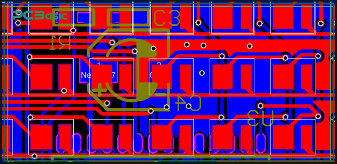
Understanding the structure of PCB layers is helpful for determining the complexity and application of the circuit board. According to the number of conductive layers, printed circuit boards are classified into three types: single-layer, double-layer and multilayer PCBs.
A single-layer PCB has only one side with a copper layer and is also known as a single-sided board. Its structure is simple and is usually composed of a copper layer, insulating materials and silkscreen. Due to having only one conductive layer, the routing space is limited and it is not suitable for complex or high-speed applications.
A double-layer PCB has copper traces on both the top and bottom surface of the circuit board, with the two PCB layers re-connected by vias. Its structure consists of a copper layer, substrate and another copper layer. Usually, plated through holes are used to achieve the conduction between the top and bottom layers. Compared with single-layer boards, it offers more flexible routing and is suitable for circuits of medium complexity. However, it still has limitations in terms of signal integrity and high-frequency performance.
Multilayer PCBs contain three or more conductive copper layers. They are alternately stacked with insulating layers and laminated into a single structure through lamination processes. Multilayer circuit boards can offer higher routing density and are commonly found in fields with extremely high-performance requirements, such as high-speed computing, medical devices, smartphones, and aerospace. However, the process of multilayer PCB manufacturing is more complex, with higher costs, longer processing cycles, and stricter requirements for design and inspection.
The primary components of a multilayer PCB include:
• Inner copper layers (signal routing or planes)
• Prepreg and core layers (insulation and support)
• Vias (through-hole, blind, or buried) to connect the PCB layers
• Solder mask and silkscreen on outer layers
To achieve a stable and reliable multilayer PCB design, a balance must be struck among performance, manufacturability and cost. The following are several key aspects:
Signal Layer Management
When designing the PCB layer structure, the positions of the signal layer, power layer and ground layer should be reasonably arranged. A common approach is to sandwich the signal layer between the ground layers, which can reduce signal interference and improve signal quality.
Via Strategy
In multilayer PCBs, different layers need to be connected through vias. When designing, through holes, blind holes or buried holes can be selected based on the structure of the board and the budget. Choosing the right through-hole type helps save space and control manufacturing costs.
Controlled Impedance
For high-speed signals, impedance matching is very important. Impedance is affected by trace width, layer spacing and the dielectric constant of the material. A good multilayer PCB design requires precise control of these parameters to ensure stable signal transmission.
Design for Manufacturability (DFM)
To simplify production, process limitations should be taken into consideration during the design. For example, it is necessary to ensure that the layers can be precisely aligned with each other, the drilling dimensions meet the requirements, and the trace spacing is reasonable. Following the DFM design principles can reduce the error risk and improve production efficiency.
CAD Tools
The use of appropriate software tools can greatly improve design efficiency. Software such as Altium, KiCad, and Cadence support stackup configuration, routing check, and electrical rule validation and are reliable multilayer PCB manufacturing and design platforms.
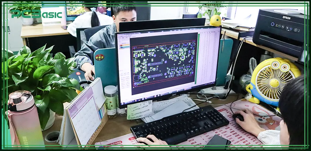
In multilayer PCB boards, the stackup refers to the arrangement and functional distribution of each layer. A reasonable stackup design not only affects the transmission quality of signals but also influences the mechanical strength and manufacturing difficulty of the circuit board. A good stackup design is a basis for achieving high-performance and high-reliability multilayer printed circuit boards.
When planning a multilayer PCB stackup, the following aspects need to be given particular attention:
Symmetrical Design
The stackup should be as symmetrical as possible. For example, the distribution of copper on the top and bottom layers should be balanced. This can effectively prevent board warping caused by uneven heating during the multilayer PCB manufacturing process.
Prepreg and Core Material Selection
Different materials will affect the dielectric constant and thermal stability of the board. Selecting the appropriate prepreg and core materials helps ensure signal speed and overall thermal stability. This is an indispensable part of multilayer PCB design.
Power and Ground Plane Layout
In the design, the placement of power and the ground layer should be carefully arranged, and it is best to be placed close to the signal layers. This can provide a stable return path for signals, reduce interference and improve signal integrity.
Interlayer Spacing Control
The distance between different layers directly affects impedance control and electromagnetic compatibility. Smaller spacing can enhance coupling and reduce crosstalk. But at the same time, the balance between manufacturing capacities and electrical performance should also be considered.
An optimized multilayer PCB stackup can effectively enhance the performance of the circuit. For any electronic product that requires high frequency, high speed or high reliability, the design of the stackup is a key step.
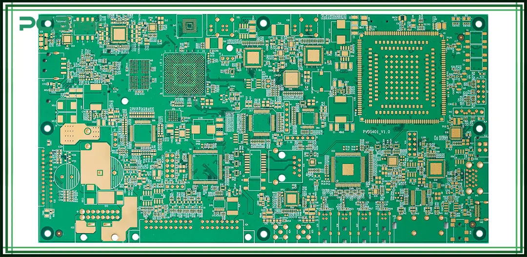
The complete multilayer PCB manufacturing process involves multiple high-precision steps. It is based on the manufacturing of single-layer or double-layer PCBs and adds the processing of inner-layer circuit preparation and multilayer lamination. Compared with ordinary boards, the production of multilayer circuit boards is more complex and has higher requirements for process control. The following is a typical multilayer PCB manufacturing process:
Inner Layer Circuit Fabrication and Etching
First, copper foil is laminated onto an insulating core material. Photolithography is used to transfer the circuit pattern onto the copper foil, and chemical etching is then applied to remove excess copper, leaving only the required traces. After this step, each inner layer circuit is completed.
Lamination and Alignment
All prepared PCB layers are stacked according to the designed stackup structure. High temperature and high pressure are used to laminate these layers into a single unified board. Precise alignment of each layer is critical to avoid errors in later stages.
Drilling and Copper Plating
Holes are drilled through the laminated board to establish electrical connections between different PCB multilayers. Then, a layer of copper is deposited on the hole walls through chemical plating, creating conductive pathways between layers. This step directly affects the reliability of electrical connections.
Outer Layer Circuit Fabrication
The process for the outer layer is similar to that of the inner layers. Photolithography is used to transfer the pattern, followed by etching to form the final outer circuits. After this step, the board’s circuitry is nearly complete.
Solder Mask and Silkscreen
A layer of solder mask ink is applied to the board’s surface to protect non-soldering areas from contamination or short circuits. Silkscreen printing is then used to add markings for component placement, company logos, and other identifiers.
Surface Finishing
Finally, the exposed pad areas undergo surface finishing. Common techniques include ENIG (Electroless Nickel Immersion Gold) and HASL (Hot Air Solder Leveling). These finishes improve solderability, prevent oxidation, and enhance corrosion resistance.
 About PCBasic
Time is money in your projects – and PCBasic gets it. PCBasic is a PCB assembly company that delivers fast, flawless results every time. Our comprehensive PCB assembly services include expert engineering support at every step, ensuring top quality in every board. As a leading PCB assembly manufacturer, we provide a one-stop solution that streamlines your supply chain. Partner with our advanced PCB prototype factory for quick turnarounds and superior results you can trust.
Choosing an experienced multilayer PCB manufacturer is critical to ensuring the quality, delivery time, and performance of your circuit boards. The manufacturer’s capabilities directly affect the stability of your product and the overall progress of the project. When selecting a partner, consider the following aspects:
• Capabilities: Can they support complex multilayer PCB board designs, including HDI and fine-pitch?
• Certifications: ISO 9001, IPC standards, RoHS compliance
• Equipment: Modern facilities for laser drilling, X-ray registration, and AOI inspection
• Lead Time: Fast turnaround for prototyping and production
• Support: Engineering feedback and multilayer PCB design review
A reliable manufacturer can help optimize your multilayer PCB fabrication and reduce time-to-market.
At PCBasic, we focus on high-precision multilayer PCB manufacturing with over 10 years of experience in engineering and project management. Our advanced equipment and skilled team allow us to deliver reliable multilayer circuit board solutions for industries like medical, automotive, industrial control, and consumer electronics.
Strong Technical Team
Our PCB design and project teams each have 10+ years of experience. We also work with PhD research teams from top universities to improve multilayer PCB design and material performance.
Flexible Production Capacity
• Shenzhen factory: Ideal for high-mix, low-volume multilayer PCB prototyping.
• Huizhou factory: Designed for cost-effective, high-volume multilayer PCB manufacturing.
In-House Manufacturing Support
We own our stencil and fixture production lines, offer CNC precision machining, and provide 1-hour stencil delivery. This helps speed up and support complex multilayer board assembly.
Reliable Component Supply
Our smart central warehouse ensures all components are original and in stock. With our one-click BOM import and instant quote system, customers can easily manage the multilayer PCB fabrication process.
Certified Quality Assurance
PCBasic is a national high-tech enterprise with certifications including ISO 13485, IATF 16949, ISO 9001, ISO 14001, and UL. We are an IPC member and hold over 20 patents related to quality inspection and production management systems.
Whether you need a 4-layer prototype or a 12-layer production order, PCBasic is your trusted partner for fast, reliable, and scalable multilayer printed circuit board manufacturing.
In today’s fast-moving and highly integrated electronics industry, multilayer PCBs have become a core technology. With higher layer density and better electrical performance, multilayer printed circuit boards are used in many electronic products—from consumer devices to industrial systems.
To use them successfully, you need the right approach. That means proper multilayer PCB design, a well-planned stackup, and a reliable multilayer PCB manufacturing process.
Whether you're working on a 4-layer PCB for a wearable device or a 12-layer server motherboard, choosing the right multilayer circuit board strategy and the right manufacturing partner is key to your project’s success.

Assembly Enquiry
Instant Quote
Phone contact

+86-755-27218592
In addition, we've prepared a Help Center. We recommend checking it before reaching out, as your question and its answer may already be clearly explained there.
Wechat Support

In addition, we've prepared a Help Center. We recommend checking it before reaching out, as your question and its answer may already be clearly explained there.
WhatsApp Support

In addition, we've prepared a Help Center. We recommend checking it before reaching out, as your question and its answer may already be clearly explained there.