Table of Contents
1. Why Does Communication Equipment Need Tighter PCB Assembly
Control?
2. What Should
Buyers Confirm Before Telecom PCB Assembly?
3. What Should Buyers Send Before a 5G or IoT
Gateway PCBA Order?
4. How Does SMT PCB Assembly Affect Reliability?
5. How Can PCBasic Support Communication PCBA Manufacturing?
6. Conclusion
7. FAQs
If you are working on a 5G
base station or IoT gateway PCB assembly project, you should not only consider
the surface mounting capability when choosing a supplier. You also need to
verify whether they can assist you in controlling the high-frequency areas, SMT
process, component sourcing, test records and the stability of repeated
production. Just because the board can pass a simple bench test does not mean
it will be stable in the future. If the impedance, welding, heat dissipation or
batch records are not managed properly, the product may still have problems in
actual use.
For this type of PCBA order, a
BOM alone is not enough. The RFQ should include clear production files, locked
component rules, inspection points, and test requirements from the beginning. This
is why communication PCBA projects are more suitable for choosing suppliers
that can manage the entire process including PCB manufacturing, component
procurement, PCB assembly, testing and post-assembly.
PCBasic, as a full-process PCB and PCBA manufacturer, can
provide support for 5G modules, IoT gateways, routers, communication
controllers and wireless communication PCBA projects. For such projects, quick
quotations are of course important, but what's more crucial is whether the
supplier can maintain a stable production process from samples to repeat
orders.
Why Does Communication Equipment Need Tighter
PCB Assembly Control?
5G base station boards and IoT gateway boards,
usually concentrate RF, high-speed signals, power supply, connectors, shielding
structure and firmware functions on the same PCBA. The more focused the board's
functionality, the more we need to pay attention to when producing. Small
problems with replacement materials, solder joints, connectors, or test steps
that may not be visible from the outside but it may affect communication
stability in actual use.
So, you don't need to make every order complicated,
but before mass production, you should tell the supplier the key risk points
that can easily affect signals, material replacement and test results, so that
the problem is not exposed until the testing or actual use stage.
High-Frequency
Areas Need Early Process Review
If you have RF modules,
antennas, filters, high-speed connectors, or communication chips on your board,
these high-frequency areas are best reviewed by the supplier before production.
Because signal stability does not depend only on the design, the assembly
process will also affect the final effect.
For example, solder joint
quality, component orientation, number of re-treatments, connector fixing
method, and whether the inspection covers the critical position will all affect
the signal path. So, you need to explain in advance which areas are sensitive
to signals and which materials cannot be replaced at will. Once suppliers have
this information, they can make advance arrangements for process, inspection
and material control. For this type of project, high-frequency
PCB processing
experience is not a simple plus, but will directly affect whether the
subsequent signal can be stable.
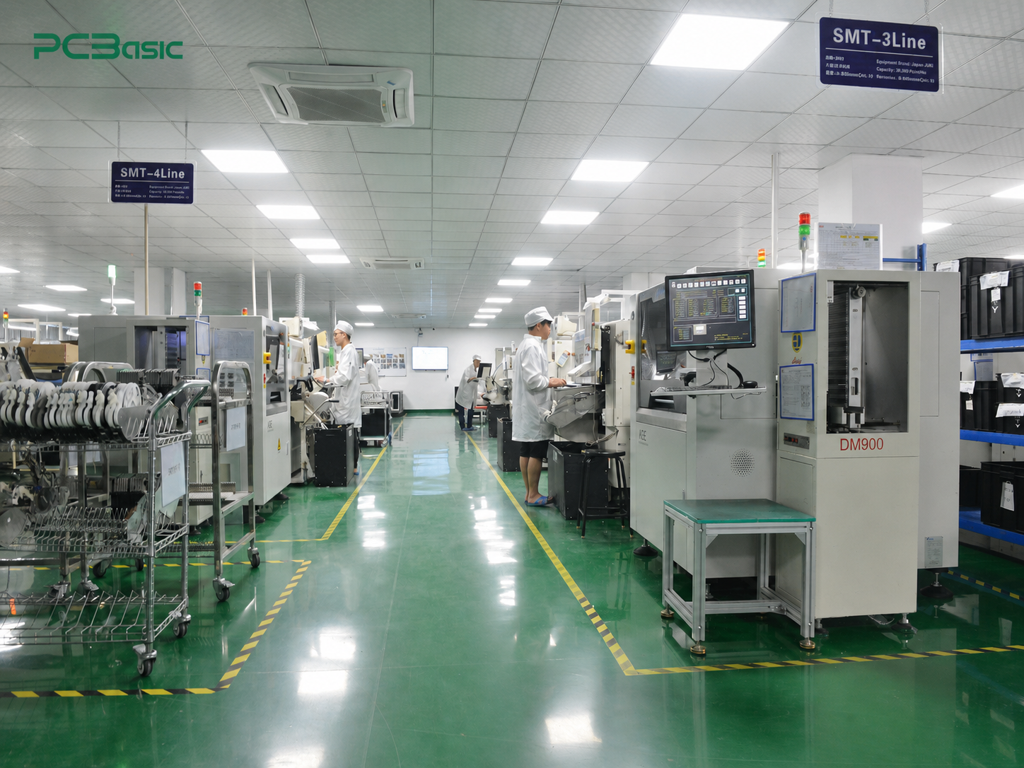
Dense SMT Layouts Need Repeatable Control
Compact gateways and
communication modules usually have limited the board subspace, but they may still
have SMT components, fine-pitch ICs, memory, RF shields, connectors and power
devices on it. For this type of SMT PCB assembly project, it's not enough for
the supplier to just say "We can mount the components." You should be
aware of a few particular issues:
• Whether solder paste
printing is checked;
• How to ensure the
mounting accuracy;
• Whether the reflow weld
curve will adjust to the plate and device;
• Check with AOI, X-ray,
or some other method to inspect after reflow.
These issues may appear to be small
production details, but in a dense SMT layout, even bridging, insufficient
solder, component shift, weak solder or hidden solder joint defects may affect
the subsequent communication function and batch stability. So, you need to
confirm these clearly before production to determine whether the supplier has a
stable SMT Assembly process.
What Should Buyers Confirm Before Telecom PCB Assembly?
If you are working on a 5G base station or IoT
gateway PCB assembly project, when making the quotation, do not just send the
PCB files to the supplier. Besides the BOM, Gerber, coordinate files and
assembly drawings, you also need to inform the supplier of several key points
in advance:
• Whether solder paste printing is checked;
• Which materials cannot be substituted;
• Which RF, high-speed or SMT areas require
special inspection;
• What tests should be conducted before
shipment;
• Which versions and production records should
be retained during the return order process.
These details do not need to be written in a
complicated way, but they must be clearly stated. The earlier the suppliers
understand these requirements, the easier it will be for them to assess the
actual production difficulty, and the quotations will be more accurate. The
material procurement, SMT assembly and testing arrangements will also be more
stable. Otherwise, later on, there is a high possibility of temporary material
changes, missed inspections, unclear testing standards, version mismatches, and
ultimately, rework or delay in delivery.
Among them, the factor that has the greatest impact
on procurement, delivery schedules, and product stability is the locking of
materials.
Locked
Components Should Be Marked Clearly
There are several types of materials on
communication circuit boards that cannot be replaced at will, such as specific
ICs, RF modules, crystal oscillators, connectors and power supply devices. They
may appear to be just one model in the BOM, but after material replacement,
they may affect signal quality, firmware compatibility, product certification,
and even whole-machine assembly.
Therefore, if you have specified materials in your
project, be sure to clearly mark them in the BOM in advance: which materials
cannot be replaced and which can be replaced; if you want to use replacement
materials, what conditions must be met and who will finally confirm them. These
rules are made clear before procurement starts, so that suppliers can judge the
risk of material shortages in advance when conducting material preparation and
BOM reviews.
Don't wait until the material is no longer
available to find a replacement. That would not only be liable to delay the
delivery date, but might also cause problems for subsequent testing and
assembly.
Testing Should
Follow Real Device Behavior
Many people will first look at
the AOI results to determine the quality of the PCBA. If the AOI is passed, it
indicates that the appearance and soldering issues have been checked, but it
cannot prove that the board is truly functioning properly. For telecom PCB
assembly, whether it can be powered on stably, whether the interface responds,
and whether the basic communication is normal, these still need to be confirmed
through testing.
Therefore, before production,
you need to communicate with the supplier clearly: which functions need to be
tested before shipment, and what results would be considered as passing. Moreover,
the testing does not necessarily have to fully replicate the real network
environment, but key functions must not be omitted.
These requirements should be
set in advance. Only then will the suppliers not merely perform a simple
power-on check, but be able to determine based on clear standards whether each
board can be shipped.
What Should Buyers Send Before a 5G or IoT
Gateway PCBA Order?
After confirming the key
requirements, your next step is to send the production materials to the
suppliers. For 5G base station or IoT gateway PCB assembly projects, only
Gerber files and BOM is usually not sufficient. You also need to let the
supplier know a few key requirements for this board: how to attach it, how to
test it before shipping, and whether there are any special requirements for the
firmware. If there are shielding covers, connectors, or housing space
limitations, please specify in advance.
If this information is not
clearly stated in the early stage, the problem will not disappear, but will
only be exposed later. For example, if the testing requirements are not clearly
explained and the structural space is not clearly explained, it may become a
new problem in the proofing, testing or assembly stages. At that time, if you
add more information and change the plan, it will easily affect the delivery
date.
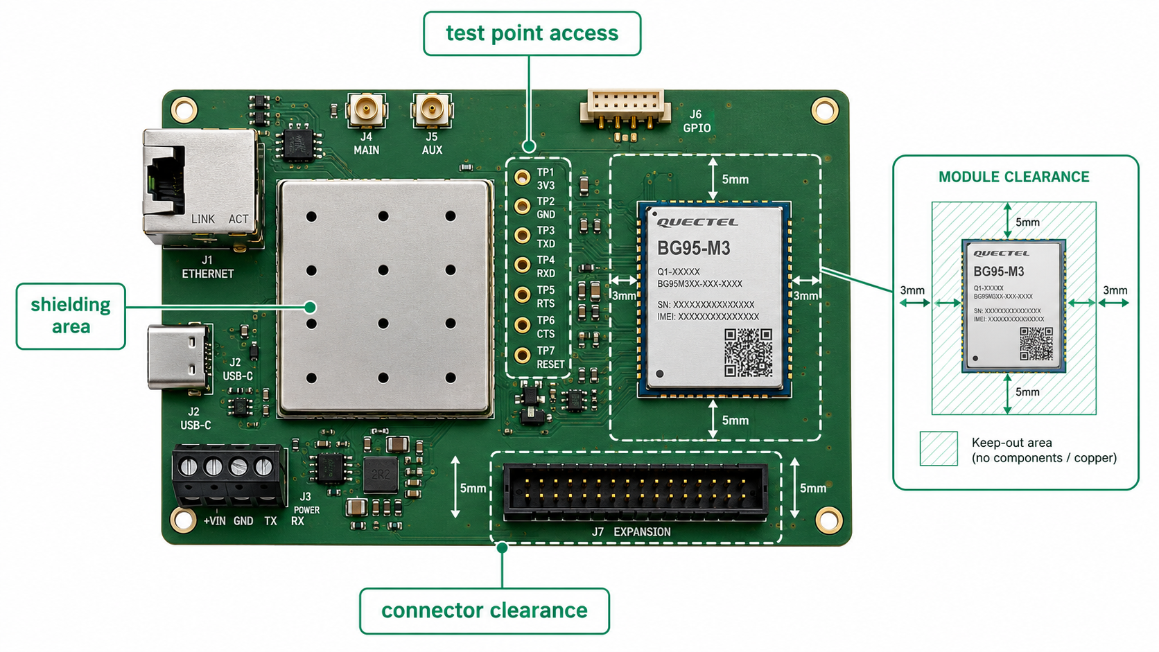
Design for
Manufacturability Review Should Include Test and Shielding Access
Design
for Manufacturability (DFM) reviews
should not only focus on PCB manufacturing and component mounting. For
communication circuit boards, you also need to let the supplier confirm in
advance that there are several areas where problems are likely to occur:
whether the test point can still be reached behind it, whether the connector is
easy to plug and unplug during testing, whether the shield will block the
inspection position, and whether there is enough space around the module.
Some test pads appear fine in
the bare board state, but may be blocked after adding the shield or completing
assembly. The connector may appear to be in the right place in the CAD, but it
may not be easy to plug and unplug during actual testing. Going through these
issues before production can reduce late revisions, manual processing and
unnecessary delivery delays.
Supplier
Review Should Start Before the Batch Is Urgent
The most worrying aspect of
the PCBA project is not the occurrence of problems, but the fact that there is
no time to make adjustments when problems arise. In many cases, the samples
have already been delayed, and only then do the customers start to provide
additional information, modify the design, and look for new suppliers. At this
point, the suppliers may still be able to help, but there is not much time left
for the adjustments of procurement, layout, fixtures, and inspection.
If your board involves high
frequency areas, high density SMT PCB assembly, special material sourcing, or
wireless communication PCBA testing requirements, it is best to inform the
suppliers of these details earlier. For projects with repeated problems in the
samples, the next step is usually not to find a fast quote from another
supplier, but to first organize the manufacturing data package clearly and have
the supplier conduct a review for you based on the complete PCBA manufacturing
process.
How Does SMT PCB Assembly Affect Reliability?
The SMT PCB assembly of
communication equipment cannot be treated merely as a routine soldering
process. For gateway boards with high-speed signals, multiple interfaces, RF
areas and compact heat dissipation paths, even a very small soldering defect
may affect the subsequent functional testing and product stability.
Therefore, you need to ensure
that the supplier has controlled the SMT process in stages rather than waiting
until the board is completed before identifying problems through testing. For
each step, such as stencil printing, placement, reflow soldering, and
post-reflow inspection, there should be corresponding confirmation and
inspection. Only in this way can defects be stopped as early as possible before
they escalate into complex rework.
Solder Paste
Control Comes Before Placement Accuracy
The solder paste application
process is when a lot of SMT welding issues actually occur. Overuse of solder
paste can lead to bridging; underuse can result in weak solder joints; and
uneven application can impact RF module pads, fine-pitch components, QFN, and
BGA areas.
As a result, while producing
high-density communication boards, you should question the supplier beforehand:
Will the solder paste in key areas be inspected prior to mounting process? SPI
(Solder Paste Inspection) can detect issues such as the volume, area, height
and offset of the solder paste before reflow soldering. Rather than waiting
until after reflow or even during the testing stage to trace soldering
abnormalities, it is better to stop the solder paste problems before mounting.
The earlier the problem is discovered, the easier it will be to control later.
AOI and X-Ray
Should Match the Risk
After reflow soldering, AOI
primarily looks for visible assembly and soldering problems. X-ray is more
suitable for inspecting hidden solder joints, such as those at the bottom of
BGA components or the bottom-terminated components. Asking the supplier,
"Have you conducted quality checks?" is insufficient. Rather, you
have to confirm the specific degree of inspection needed for this board.
Before production, you should
verify the inspection plan with the supplier if your board has BGA components,
shielding modules, dense connectors, or solder joints that are difficult to see
with the unaided eye. The hazards are
different for a high-speed base station module and a fundamental IoT gateway,
so the test depth shouldn't be the same. You should make it clear before
production if the area needs X-ray inspection.
Rework Rules
Should Be Clear
Rework is occasionally unavoidable throughout the
sample and pilot production phases. However, the quality concerns would greatly
increase if rework is done frequently close to RF lines, fine-pitch integrated
circuits, or heat-sensitive modules.
Therefore, prior to production, you must agree with
the supplier the rework guidelines, including which circumstances permit
rework, how the reworked boards should be re-inspected, and when rework should
cease and the boards should be deemed trashed. Even if the quotation is later
reduced, it will be challenging to counter these quality concerns if the
revised boards are not recorded individually and are even included with regular
boards.
How Can PCBasic Support Communication PCBA Manufacturing?
When selecting a supplier for a 5G base station or
IoT gateway PCB assembly project, you need take into account more than just
their soldering skills. You also need to check whether the various processes
such as data collection, materials, production and testing can be smoothly
connected, because this is often the key factor that affects the stability of
delivery.
These processes are handled in the same workflow by
PCBasic's PCB
assembly services. Together, we
examine the BOM, process specifications, test plans, and production records in
addition to finishing SMT PCB assembly. We may detect hazards in materials,
processes, testing, and traceability earlier rather than waiting until the
production or testing phases when these issues become apparent.
MES
Traceability Helps Repeat Orders
Before the wireless
communication PCBA is finalized, it is often revised several times. Maybe this
time the firmware was updated, next time the connectors were changed, later on
the substitute materials were confirmed, or the module supplier was replaced.
If these changes are only
recorded in emails, they may seem fine in the short term. But when it comes to
reordering, reworking, or problem investigation, things can easily get messy.
Without clear records, it will be very difficult to quickly confirm later.
Therefore, what you need is
not just the delivery records after production is completed, but a process that
can trace the orders, batches, materials, tests and rework situations. Only in
this way can you quickly confirm the following key information during the
subsequent verification process:
Build records
• the
BOM version used for production
• the
component lot used in the build
• the
firmware version loaded
Quality records
• the
inspection step where the issue was found
• the
boards that were repaired and retested
Repeat-order records
• the
batch that should be repeated for the next order
In PCBasic, the quality
control system MES is not
only used for production scheduling. It also records key data during the PCBA
production process, such as material batches, inspection results, production
status, and final test results.
When your project enters the
repetitive production stage, these records become very important. We can trace
each production situation by order and batch, and confirm what materials were
used, what inspections were conducted, and what the test results were for this
batch of boards.
If there is a need for rework,
troubleshooting, or version confirmation later, there is no need to go through
emails, search for tables, or piece together documents. Many of the information
can be directly retrieved from the corresponding orders and batches.
Related
PCBasic Guides Support Broader Review
Communication-related PCBA
projects usually involve more than just the soldering of one board. If you want
to learn about the complete process from document review, material preparation,
SMT assembly, testing to shipment, you can continue reading the PCBasic’s guide
on the electronic
manufacturing process.
If you are comparing flying
probe testing, ICT testing and FCT functional testing, you can also check the
PCBasic’s PCBA testing guide to determine which testing combination is more
suitable for your product.
These contents can help you
examine the project from different perspectives: communication PCB assembly
focuses more on application scenarios and delivery requirements; SMT assembly
focuses more on the soldering and assembly process; high-frequency PCB focuses
more on signal sensitive areas; and quality control focuses more on production
records and traceability. This way, when looking for a supplier or preparing
RFQ materials, you will be clearer about which issues need to be confirmed in
advance.

Conclusion
The PCB assembly of 5G base
stations and IoT gateway devices cannot be handled merely by conventional
circuit board soldering. Factors such as the high-frequency area, dense SMT
layout, key communication components, test plans, and production traceability
all affect the stability and reproducibility of subsequent production.
If these requirements are not
clearly confirmed before production, problems often do not surface immediately
but are revealed during testing, assembly, rework, or re-submission. For the buyers,
truly reliable communication-type PCBAs are not just about manufacturing the
boards, but ensuring that the materials, processes, tests, and records of each
batch of boards can all be controlled.
PCBasic can provide services
for high-frequency PCB manufacturing, SMT assembly, PCB assembly, component
procurement, testing, and MES quality record support. If your project involves
RF modules, dense SMT layout, locked communication components, or wireless communication
PCBAs with test requirements, you can submit PCB files, BOM, and production
issues to Contact
Us to have PCBasic assess the manufacturing risks for you first.
FAQs
Q1: What makes 5G base station PCB
assembly different from normal PCB assembly?
A1:
It often involves high-frequency signal paths, dense SMT PCB assembly, stricter
component control, and testing linked to communication performance.
Q2: What should buyers prepare for
telecom PCB assembly?
A2:
Buyers should prepare Gerber files, BOM, pick-and-place data, RF notes, testing
needs, firmware notes, and locked component information.
Q3: Why is traceability important for
wireless communication PCBA?
A3:
Traceability helps buyers connect BOM versions, component lots, inspection
records, firmware versions, and test results across repeat batches.