Global high-mix volume high-speed PCBA manufacturer
9:00 -18:00, Mon. - Fri. (GMT+8)
9:00 -12:00, Sat. (GMT+8)
(Except Chinese public holidays)
Global high-mix volume high-speed PCBA manufacturer
9:00 -18:00, Mon. - Fri. (GMT+8)
9:00 -12:00, Sat. (GMT+8)
(Except Chinese public holidays)
HomePage > Blog > Knowledge Base > Industrial PCB: A Complete Guide
PCB is the foundation of modern electronic products. Today, we are going to talk about one of the branches within this overall system - industrial PCB.
In the vast field of circuit boards, the industrial PCB can be regarded as the most demanding and crucial sub-sector. Industrial equipment has extremely high requirements for industrial circuit boards. Not only do they need to be precise, but they also need to be "robust" (able to operate stably for a long time).
Next, in this guide, we will take you through a comprehensive understanding of industrial PCBs. First of all, let's start by learning about its definition.
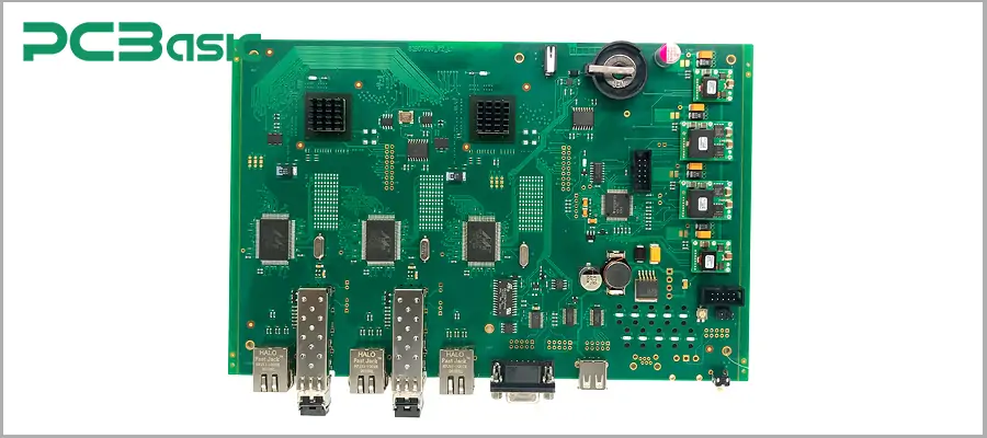
An industrial PCB is, in simple terms, a circuit board specifically designed for industrial environments. It is different from the circuit boards found in common consumer electronic products. It does not aim for small size and low cost. Instead, it focuses on the requirements for stable operation, safety, and reliability in harsh environments.
Industrial PCBs are commonly used in industrial automation, robotics, automotive systems, power and energy, communication equipment, aerospace, and high-end medical equipment. Their most notable feature is their ability to operate stably in various complex and even harsh environments, such as:
1. High durability: Industrial PCBs typically have thicker copper layers, stronger substrates, and more robust solder mask. This enables them to withstand temperature fluctuations, electrical shocks, and mechanical stress.
2. Long-term reliability: Industrial PCBs are designed for long-term stable operation. Their lifespan and reliability are much higher than those of ordinary circuit boards. This is precisely why they are widely used in applications where errors are unacceptable, such as aerospace navigation, factory automation control, or life support medical equipment.
3. Compliance with strict standards: Industrial PCBs are manufactured according to strict international standards, such as IPC Class 3, IPC-6012, IPC-A-610, IEC-61188, UL 796, etc. These standards ensure the quality, safety, and consistency of the circuit boards, allowing the products to smoothly enter the global market.
Without industrial PCB manufacturing, many of our modern devices might not function properly. They are the "nerve centers" of industrial electronic systems and one of the most crucial links in the entire circuit board industry.
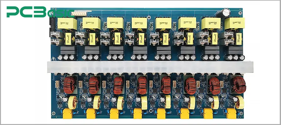
The requirements for circuit boards in industrial applications are far higher than those for consumer products. It is not only necessary for industrial PCBs to function properly, but they must also comply with strict international standards. If the design is not up to par, they may still work in the short term, but they simply cannot withstand the harsh industrial environment.
In every stage of industrial PCB manufacturing - from material selection to assembly - international standards set by organizations must be followed. The significance of these standards lies in consistency, compatibility, safety and reliability.
If standards are not followed in industrial PCB production, it may lead to very serious consequences: equipment failure, product recalls, legal risks, safety accidents, etc. The following are several international standards that have the greatest impact on industrial PCB design and manufacturing:
|
Standard |
Description |
Application in PCB Industry |
|
IPC Class 3 |
Defines requirements for high-performance electronics with zero tolerance for failure |
Used in aerospace, defense, medical devices where reliability is critical |
|
IPC-6012 |
Specifies qualification and performance for rigid PCBs |
Common in automotive systems and industrial control boards |
|
IPC-A-610 |
Sets acceptability criteria for electronic assemblies |
Ensures assembly processes meet consistent quality benchmarks |
|
IEC-61188 |
Governs the design, layout, and documentation of printed boards |
Provides global consistency for PCB designers |
|
UL 796 |
Standard for safety and fire resistance of printed-wiring boards |
Ensures industrial PCBs can handle high voltages and harsh conditions |
Material selection is crucial in PCB manufacturing. Only with the right materials can a PCB achieve its intended purpose. This is also true for industrial PCBs.
Common industrial PCB production materials include:
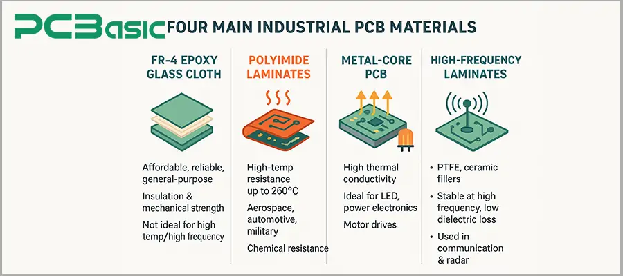
FR-4 epoxy glass cloth: Made of fiberglass and epoxy resin, this material is affordable and highly reliable, making it the most widely used material in the PCB industry. It strikes a balance between performance and cost, making it ideal for general-purpose industrial PCBs. While this material may perform poorly in high-temperature or high-frequency applications, products made with it offer balanced performance, including excellent insulation and mechanical strength.
Polyimide laminates: This material is renowned in the PCB industry for its high-temperature and chemical resistance. It can withstand temperatures as high as 260°C, making it popular in applications requiring high-temperature resistance, such as aerospace, military, and automotive electronics. Furthermore, this material offers excellent flexibility and strong mechanical properties.
Metal-Core PCBs: These use a metal substrate that dissipates heat much better than conventional laminates. Their excellent thermal conductivity makes them ideal for high-power circuits and LED lighting. Common applications using industrial PCBAs include power electronics, motor drives, and energy conversion systems.
High-frequency laminates are commonly found in communications equipment, radar, and other high-end industrial PCB designs. These laminates, made of materials like PTFE or ceramic fillers, are often used for high-frequency circuits. They offer exceptional stability in high-frequency applications, low dielectric loss, and high signal integrity.
Like other PCBs, industrial PCBs come in a variety of structures to suit various applications.
|
Structure Type |
Description |
Typical Industrial PCB Applications |
|
Single-layer / Double-layer PCBs |
Basic boards with one or two copper layers, simple design and cost-effective. |
Sensors, power supplies, general-purpose industrial PCB assembly |
|
Multi-layer PCBs |
Multiple conductive layers laminated together, enabling complex routing. |
Automation systems, robotics, medical electronics |
|
Rigid-flex PCBs |
Combination of rigid and flexible sections, offering mechanical adaptability. |
Complex environments, aerospace, defense, advanced industrial devices |
An effective industrial PCB design must balance long-term dependability, performance, and manufacturing feasibility. A good design makes the industrial PCB manufacturing process easier while also guaranteeing great functionality. Additionally, it enhances the long-term dependability of industrial PCB assembly and lowers manufacturing errors. We've outlined a number of things to think about while creating circuit boards for challenging conditions below.
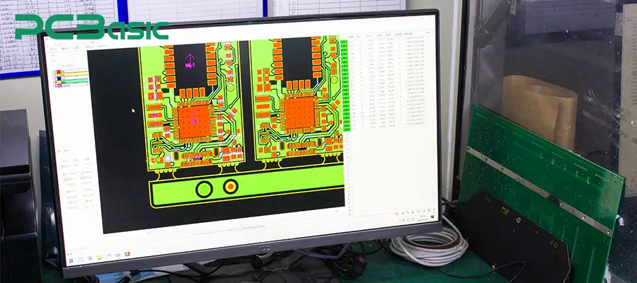
1. Pay attention to signal integrity during the design process. Signal integrity is one of the most important aspects of industrial PCB design. Poor signal integrity can lead to data errors, noise, and failures. We can use controlled impedance routing to match the electrical characteristics of the signal; or optimize the stackup of multilayer boards to minimize crosstalk and electromagnetic interference; or improve the stability of high-speed designs by using ground planes and shielding.
2. Copper thickness and current carrying capacity. Current carrying capacity is crucial for power electronics, automotive systems, and energy devices. If traces are too thin or the copper layer is insufficient, overheating and reliability issues can occur. We can increase copper thickness to ensure safe current transmission; or optimize vias to evenly distribute current across layers.
Considering appropriate copper thickness during the industrial PCB design phase can avoid costly rework and enhance product safety.
3. Thermal management. Industrial PCBs are often exposed to high temperatures during use. Therefore, thermal management and appropriate heat dissipation measures are essential. Consider the following thermal management techniques:
Design directly impacts the performance, production yield, and total cost of ownership of the finished product. Therefore, careful consideration is essential when designing your PCB.
Industrial-grade PCB manufacturing is a multi-stage, tightly controlled, precision process. Each step is interconnected. Below, we'll explain the industrial PCB manufacturing process.
(For multilayer PCBs, the following steps typically include inner layer fabrication → AOI → black oxide (oxide treatment) / roughening → lamination.)
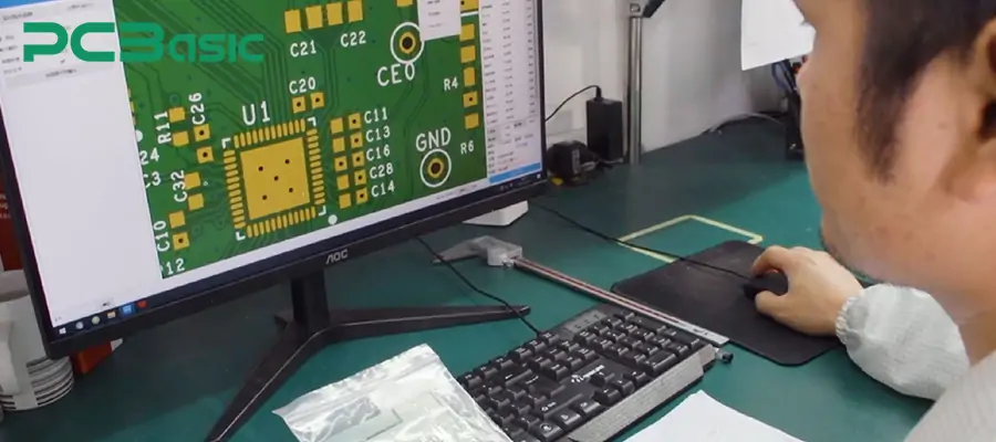
The purpose of this stage is to ensure the design is manufacturable, testable, and cost-effective.
First, a DFM/DRC check is performed. This includes checking line width/spacing, via annular ring width, impedance-controlled stackup, copper balance, panelization, fiducial markings, solder mask bridge width, character avoidance, and window size.
Next, a process capability match is performed. The drill aspect ratio, minimum solder mask bridge, minimum mechanical/laser via, laminate structure, and impedance control tolerances are confirmed to meet the factory's capabilities.
Then, testing and traceability are performed. Add test points and unique barcodes/QR codes to meet the traceability requirements commonly used in the printed circuit board industry.
The purpose of cleaning and cutting is to create a clean, flat surface for pattern transfer and electroplating. Key points include:
Chemical/mechanical methods should be used to remove contamination and oxide layers to improve copper adhesion.
Pre-baking should be performed as necessary to remove moisture and prevent blistering and delamination in subsequent steps.
Optimize panel dimensions based on production line equipment size and capacity.
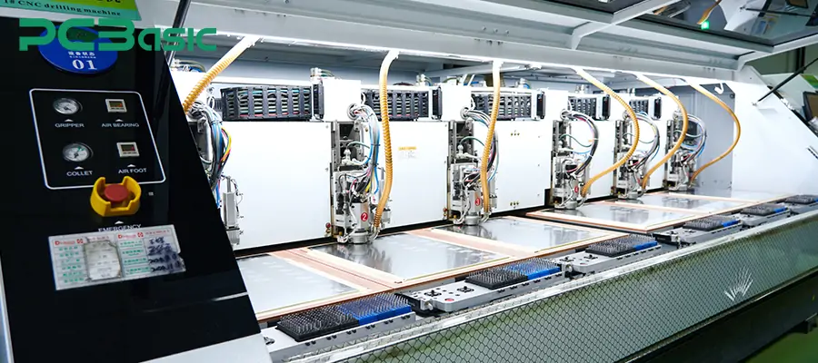
This step involves forming the required through-holes (PTHs), non-plated-through-holes (NPTHs), and micro-blind/buried vias required for HDI. Typically, mechanical drilling is used for standard holes; during the process, care should be taken to control tool wear, hole position deviation (TIR), and burrs.
Laser drilling is used for micro-blind vias (µVia).
Desmearing and plasma treatment are used to remove resin residue from the via walls and improve the quality of the metallization.
This step forms a continuous conductive layer on the hole wall and copper surface, laying the foundation for subsequent circuitry and current carrying. Key points include:
Activation (Pd/Sn) → Electroless Copper (PTH): Creates a thin conductive copper layer on the insulating hole wall.
Acidic Copper Plating (Pattern/Panel Plating): Thickens the surface and hole wall copper.
Specialty Plating: Via Fill, Resin Plug, etc.
Accurately transfer the circuit pattern to the copper surface.
Key points:
Dry Film Lamination/Inkjet Pre-solder Mask Imaging & Laser Direct Imaging (LDI)
Development removes the unexposed photoresist areas, leaving the areas to be plated/preserved as copper.
Etching removes excess copper, leaving only the traces and pads required by the design.
Key Points:
Chemical etching should be uniform.
A plating-then-etching process ensures critical conductor thickness.
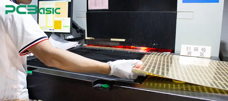
To identify defects such as shorts, opens, gaps, and offsets before interlayer synthesis or solder mask application.
Key Points:
High-resolution camera alignment: Identify defects by comparing with Gerber/ODB++ or gold samples.
Feedback loop: Close the defect loop to the front-end process for continuous yield improvement (SPC).
Apply solder mask to protect the copper surface, prevent solder bridges, and define the solderable area of the pad.
Key Points:
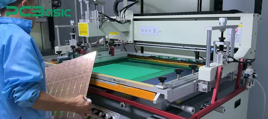
Green ink (LPI) or colored solder mask: Ideally, use a silkscreen/inkjet/LDI process. Care should be taken to control solder mask bridges and compensate for window openings.
Curing: Pre-bake + UV/thermal cure to ensure adhesion and chemical resistance.
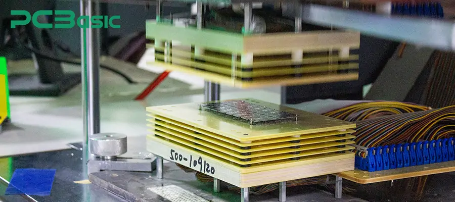
Surface treatment prevents oxidation of bare copper, improving solderability and assembly reliability. Common surface finishes include:
HASL: Low cost, suitable for general industrial PCB assembly.
ENIG: Excellent flatness, fine pitch, and BGA compatibility, commonly used in industrial and medical applications.
ENEPIG: Compatible with soldering and wire bonding, suitable for multiple assembly runs and high-reliability applications.
Other finishes include immersion silver, immersion tin, and OSP, depending on the application.
Before assembly, electrical testing is required to verify circuit functionality and insulation performance.
Key Points:
Flying Probe: Flexible, fixture-free, suitable for small batches of multiple products.
Bed-of-Nails (ICT): Fast, suitable for high-volume mass production.
Test Items: Open/short circuit, insulation resistance, withstand voltage/high voltage, and (if necessary) controlled resistance spot checks.
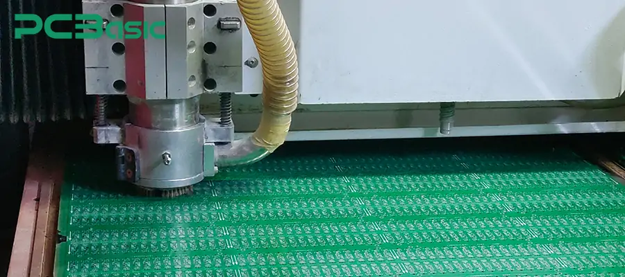
Divide the panel into the final single board outline or daughter boards to ensure proper assembly component alignment.
Key Features:
CNC milling/routing, V-cut, and tab-routing (with mouse-bites)
Chamfering, slotting, countersinking, and special-shaped edge processing to meet end-of-line assembly requirements
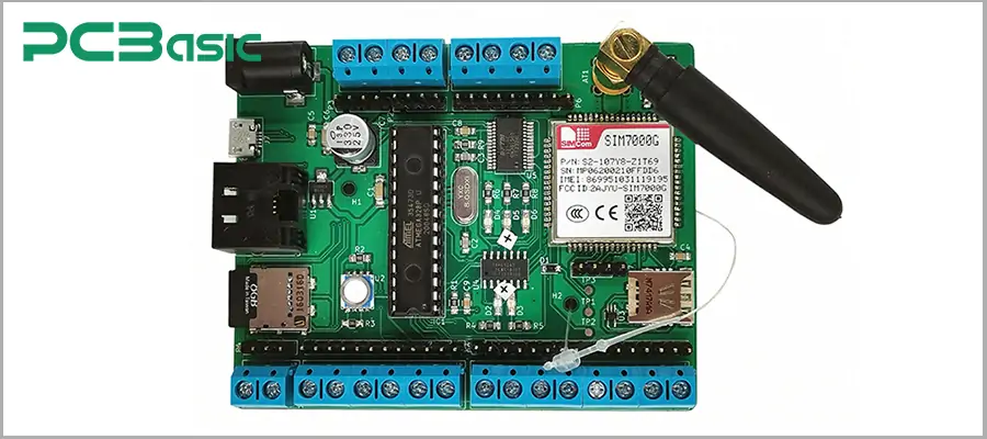
When choosing a partner for industrial PCB fabrication, important factors to take into account are:
1. Be aware of their compliance and certifications. International certifications like ISO 9001 (quality management), IATF 16949 (automotive electronics), and ISO 13485 (medical devices) are held by reputable manufacturers.
2. View their production machinery. To guarantee product accuracy, top suppliers use cutting-edge equipment including AOI, X-ray inspector, and flying probe tester. Selective wave soldering, 3D inspection systems, and nitrogen reflow are additional features of high-end production lines.
3. Inquire about their supply chain and delivery capabilities worldwide. Reputable producers provide scalable manufacturing capacity, quick development, and worldwide delivery.
4. Find out more about their long-term services and post-purchase assistance. Customers are guaranteed to gain the entire lifespan value of their investment in industrial PCB manufacture when they receive comprehensive post-sales support, which includes maintenance suggestions, failure analysis, and continuing technical service.
Automation, healthcare, energy, and automotive technology breakthroughs are largely driven by industrial PCBs. The performance and dependability of the finished industrial PCB assembly are determined at every stage, from industrial PCB design to industrial PCB manufacturing procedures and strict industry requirements. To put it briefly, industrial PCBs are the unseen engine that propels contemporary industrial innovation. They offer a strong basis for upcoming industrial development in addition to supporting the most demanding applications around the globe.
 About PCBasic
Time is money in your projects – and PCBasic gets it. PCBasic is a PCB assembly company that delivers fast, flawless results every time. Our comprehensive PCB assembly services include expert engineering support at every step, ensuring top quality in every board. As a leading PCB assembly manufacturer, we provide a one-stop solution that streamlines your supply chain. Partner with our advanced PCB prototype factory for quick turnarounds and superior results you can trust.

Assembly Enquiry
Instant Quote
Phone contact

+86-755-27218592
In addition, we've prepared a Help Center. We recommend checking it before reaching out, as your question and its answer may already be clearly explained there.
Wechat Support

In addition, we've prepared a Help Center. We recommend checking it before reaching out, as your question and its answer may already be clearly explained there.
WhatsApp Support

In addition, we've prepared a Help Center. We recommend checking it before reaching out, as your question and its answer may already be clearly explained there.