Global high-mix volume high-speed PCBA manufacturer
9:00 -18:00, Mon. - Fri. (GMT+8)
9:00 -12:00, Sat. (GMT+8)
(Except Chinese public holidays)
Global high-mix volume high-speed PCBA manufacturer
9:00 -18:00, Mon. - Fri. (GMT+8)
9:00 -12:00, Sat. (GMT+8)
(Except Chinese public holidays)
HomePage > Blog > Knowledge Base > Copper Coin PCB for Extreme Heat Dissipation
As electronic products become smaller and more powerful, the problem of heat generation on circuit boards has become more serious. High-power devices like some drivers and communication modules generate a large amount of heat in a very small area. Without proper thermal management, the heat not only causes the performance of components to decline, but also may lead to damage and affect the lifespan of the entire device.
Common heat dissipation methods, such as thermal vias, copper pours, heat sinks, or even metal core PCBs for heat dissipation, are no longer sufficient in some high-power or high-heat-density scenarios. At this point, the copper coin PCB is needed to enable heat to be directly and quickly transferred from the heat-generating components to the heat sink or the external environment, shortening the heat dissipation path and improving efficiency.
In this blog, we will introduce the copper coin PCB in detail, including its structures, type differences, design key points, possible problems encountered in the manufacturing process, and its application performance in actual high-power devices.
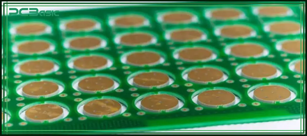
A Copper Coin PCB (copper block PCB) refers to a type of multilayer printed circuit board that embeds a solid copper block inside it, which is known as PCB copper coin or PCB coin. This piece of copper is usually designed directly underneath chips or power devices that generate a lot of heat, functioning as a thermal bridge to help heat leave components more quickly.
In a standard PCB, heat needs to pass through FR-4, an insulating material, first. Its thermal conductivity is very low, and its heat dissipation efficiency is not high either. In the copper coin PCB, the heat is directly transferred to the copper block and then rapidly transferred to the other side of the circuit board or the heat sink, with a shorter path and higher efficiency.
The reason for using copper is that its thermal conductivity is approximately 380-400 W/m·K, while that of FR-4 is only 0.3-0.5 W/m·K. That is to say, the thermal conductivity of copper is 200 to 800 times higher than that of the commonly used insulating materials for PCBs. Therefore, copper coin PCBs have become an ideal way to solve the heat dissipation problem of high-power and high-heat-density electronic products, such as in power modules, LEDs, radio frequency equipment, automotive electronics and other fields.
According to the differences in design requirements, component layout and manufacturing methods, PCB copper coins can be classified into different types:
|
Type of PCB Coin |
Description |
Visibility |
Typical Usage |
|
Buried Copper Coin |
Fully embedded inside PCB layers |
Not visible |
Internal thermal transfer |
|
Surface Copper Coin |
Exposed on the PCB surface |
Visible |
Direct interface with heat sink |
|
Through-Board PCB Coin |
Copper passes completely through PCB |
Visible both sides |
Highest cooling efficiency |
|
Press-Fit PCB Copper Coin |
PCB coin pressed into plated hole |
Slightly raised or recessed |
Lower cost, quicker process |
|
Embedded & Metallized Copper Coin |
Copper inserted into cavity then plated |
Smooth & planar |
High performance & reliability |
We can see from the table that each copper coin PCB structure provides unique advantages depending on application requirements.
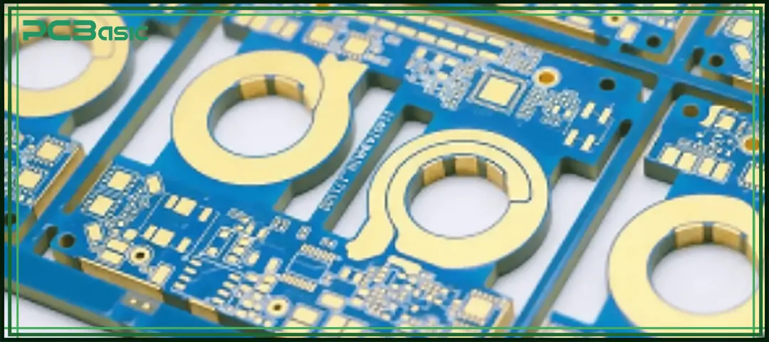
The heat dissipation mechanism of copper coin PCBs is based on the design concept of establishing a low thermal resistance path with high thermal conductivity metal materials. By embedding solid copper coins inside PCBs, heat can be directly transferred from the chip to the heat dissipation medium, which can reduce heat accumulation in insulating materials (such as FR-4), thereby enhancing the overall heat dissipation efficiency.
The heat flow in the copper coin PCB can be divided into the following stages:
1. Heat Generation
High-power chips or power devices generate heat during operation.
2. Heat Transfer from Pad to Copper Coin
Heat is conducted from the component pad to the copper coin located underneath or adjacent to the component.
3. Vertical Heat Conduction Through the Copper Coin
Due to the high thermal conductivity of copper (approximately 380–400 W/m·K), heat is rapidly conducted vertically through the PCB stack-up, bypassing the low-thermal-conductivity FR-4 material.
4. Heat Spreading or Transfer to Heat Dissipation Structures
After passing through the PCB, the heat spreads into large copper planes or is transferred to external heat sinks, aluminum bases, or metallic enclosures.
5. Heat Dissipation into the Environment
Finally, the heat is dissipated into the surrounding air via convection or conducted to the chassis or housing.
Time is money in your projects – and PCBasic gets it. PCBasic is a PCB assembly company that delivers fast, flawless results every time. Our comprehensive PCB assembly services include expert engineering support at every step, ensuring top quality in every board. As a leading PCB assembly manufacturer, we provide a one-stop solution that streamlines your supply chain. Partner with our advanced PCB prototype factory for quick turnarounds and superior results you can trust.
The power of electronic products is getting higher and higher, and the problem of heat generation must be solved. Different thermal management solutions each have their own characteristics: some have low costs but average effects, while others have strong heat conduction but are expensive. Copper coin PCBs fall between the two, providing efficient heat conduction without being as expensive as ceramic or diamond materials, making them suitable for large-scale use in industrial products.
The following table compares several common thermal management solutions to facilitate an intuitive understanding of their differences in heat conduction capacity, efficiency, cost and application scenarios.
|
Solution |
Thermal Conductivity |
Efficiency |
Cost |
Best Use Case |
|
Thermal Vias |
Low |
Basic |
Low |
Standard PCBs |
|
Copper Pour |
Medium |
Moderate |
Low |
Low-power boards |
|
MCPCB (Metal Core PCB) |
~12 W/mK |
Good |
Medium |
LED lighting |
|
Copper Coin PCB |
380–400 W/mK |
Excellent |
Medium–High |
High-power electronics |
|
Aluminum Base |
~200 W/mK |
Good |
Medium |
Automotive lighting |
|
Ceramic / Diamond |
700–2000 W/mK |
Excellent |
Very High |
Aerospace, military |
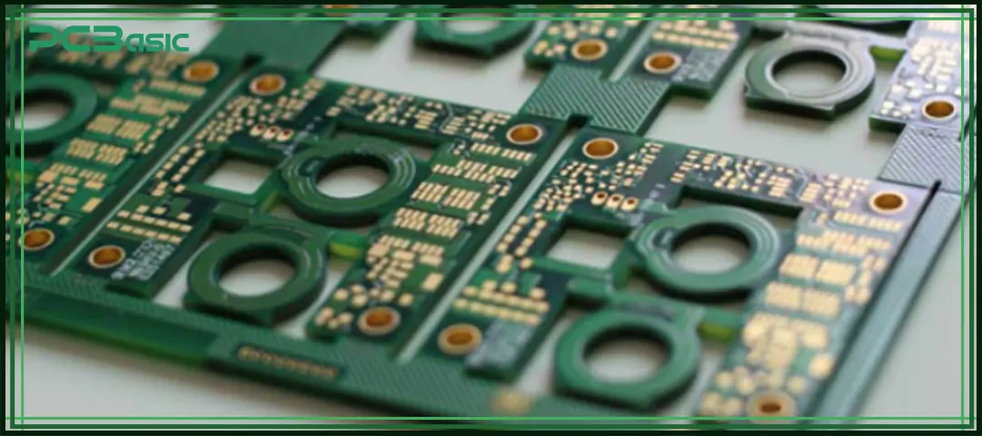
The key to copper coin PCBs lies in: where the copper blocks are placed, how the board layers are designed, and whether the processing is aligned. Only when these are handled properly can the ideal heat dissipation effect be achieved.
• The copper coin should be placed directly under the heat-generating component or as close to it as possible
• Minimize the distance between the component pad and the copper surface
• Avoid routing high-speed signal traces in this area
• Ensure the copper coin does not interfere with BGA solder balls or vias
2. PCB Stack-Up Considerations A typical copper coin PCB stack-up includes: • Solder mask and component layer • Copper pads / Thermal interface • Embedded PCB copper coin • Prepreg + Inner copper layers • Bottom copper layer or heat sink Coin shape options: • Circular • Rectangular • Step-shaped (multi-level) • Custom geometry tailored to component footprint
A typical copper coin PCB is built with the following structure:
• Top layer with solder mask and component pads
• A solid PCB copper coin embedded beneath the pad area
• Prepreg and inner copper layers underneath
• Bottom copper layer or a heatsink/metal base, depending on the design
The PCB coin itself can be circular, rectangular, step-shaped, or customized to match the component footprint.
There are three commonly used methods to embed a PCB coin into a PCB:
|
Manufacturing Method |
Basic Process |
Advantages |
Disadvantages |
|
Milling Slot + Insertion + Lamination |
Mill slot in PCB → Insert copper coin → Laminate and cure |
Strong bonding |
Complex and time-consuming process |
|
Press-Fit |
Drill oversized hole → Press copper coin into PCB |
Low cost, fast process |
Surface may not be perfectly flat |
|
Insertion + Surface Plating |
Insert copper coin → Surface plating for leveling |
Best surface flatness |
Requires high manufacturing precision |
During production, copper coin PCBs may face a few issues:
• If the coin shifts during lamination, heat transfer may be compromised.
• Resin overflow around the PCB coin can cause bumps or voids on the surface.
• Exposed PCB copper must be treated to prevent oxidation.
• The coin takes up internal PCB space, making routing more difficult—especially in high-density or HDI designs.
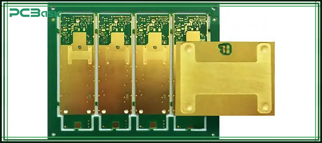
Copper coin PCBs are widely used in industries where heat dissipation performance directly affects the performance and safety of equipment.
|
Industry |
Example Applications |
|
RF & Microwave |
RF Power Amplifiers, Phased Array Tx/Rx Modules |
|
Telecom & 5G |
GaN Power Transmitters, SSPA, Base Stations |
|
Aerospace & Defense |
Radar systems, Satcom, Avionics electronics |
|
Automotive & EV |
LED headlights, Motor control, Battery BMS |
|
Power Electronics |
DC-DC converters, Inverters, High-current PSU |
|
IoT & Embedded |
Remote sensors, compact battery modules, data loggers |
The copper coin PCB is currently one of the most effective and reliable heat dissipation methods in high-power electronic devices. It forms a heat conduction path with extremely low thermal resistance by directly embedding the PCB copper coin inside the circuit board, which can transfer heat from the chip more quickly, reduce the temperature and extend the lifespan of the device.
Compared with traditional thermal vias or MCPCB metal substrates, copper coin PCBs conduct heat faster, have more uniform thermal diffusion, lower thermal resistance, occupy less space and have higher overall reliability.
As electronic devices become smaller and more powerful, the importance of this technology will continue to rise. From automotive electronics and satellite systems to 5G base stations and LED lighting modules, PCB coins have become an ideal choice for enhancing heat dissipation performance and reliability.

Assembly Enquiry
Instant Quote
Phone contact

+86-755-27218592
In addition, we've prepared a Help Center. We recommend checking it before reaching out, as your question and its answer may already be clearly explained there.
Wechat Support

In addition, we've prepared a Help Center. We recommend checking it before reaching out, as your question and its answer may already be clearly explained there.
WhatsApp Support

In addition, we've prepared a Help Center. We recommend checking it before reaching out, as your question and its answer may already be clearly explained there.