Global high-mix volume high-speed PCBA manufacturer
9:00 -18:00, Mon. - Fri. (GMT+8)
9:00 -12:00, Sat. (GMT+8)
(Except Chinese public holidays)
Global high-mix volume high-speed PCBA manufacturer
9:00 -18:00, Mon. - Fri. (GMT+8)
9:00 -12:00, Sat. (GMT+8)
(Except Chinese public holidays)
HomePage > Blog > Knowledge Base > Circuit Board Basics: Everything You Need to Know
Whether you are an enthusiast interested in electronics, a novice starting DIY projects, or a beginner entering the field of engineering, it is essential to master the circuit board basics. Circuit boards are the foundation of modern technological devices and are almost everywhere.
In this article, we will lead you to have a comprehensive grasp of the basics of circuit boards. We will explore what a printed circuit board (PCB) is, how it is manufactured, common types and materials, the fundamentals of circuit board design, PCB manufacturing and assembly processes, common testing methods, application scenarios and industry certifications, etc.
Learning the basics of printed circuit boards can enable you to master troubleshooting, create functional electronic devices, and understand the core principles of how technological products operate.
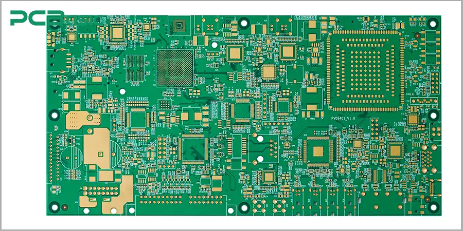
A circuit board, most commonly known as a printed circuit board, is a flat board that connects electronic components through copper wires. It is used to achieve the distribution and transmission of electrical energy and signals. At the core of every modern electronic board is a circuit board. Its main function is to allow electrical signals and power to flow among various circuit board components, such as resistors, capacitors, chips and connectors, thereby achieving a compact and reliable circuit design.
So, what role does the PCB play? The answer is: It makes today's advanced electronic products possible. Through meticulous PCB layout, power distribution and signal routing, designers ensure that all parts of the circuit board work in coordination. Without the structure and electrical frame provided by the PCB, complex functions are almost impossible to integrate into small devices.
To fully master the basics of a printed circuit board, it is also necessary to understand some common terms, which run through the entire process of electronic manufacturing and PCB design.
|
Term |
Meaning |
|
PCB |
Printed Circuit Board |
|
PWB |
Printed Wiring Board (bare PCB) |
|
PCBA |
PCB with components assembled |
|
SMT |
Surface Mount Technology |
|
THT |
Through-Hole Technology |
There are many types of circuit boards. Different design requirements, application scenarios and performance requirements determine that PCBs have various structures and forms. Below are the classifications we have made respectively based on structure, rigidity and function. Special circuit boards for specific scenarios are also listed.
Printed circuit boards can be classified into the following categories according to the number of copper layers and connection methods:
Single-sided PCB
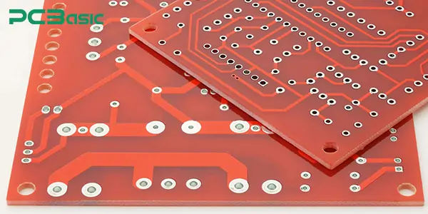
Single-sided PCB is the most fundamental type of circuit board. It is called a single-sided PCB because all components are installed on one side. It only needs simple circuit board design, a starting point for learning and mastering circuit board basics (soldering circuit board basics).
Double-sided PCB
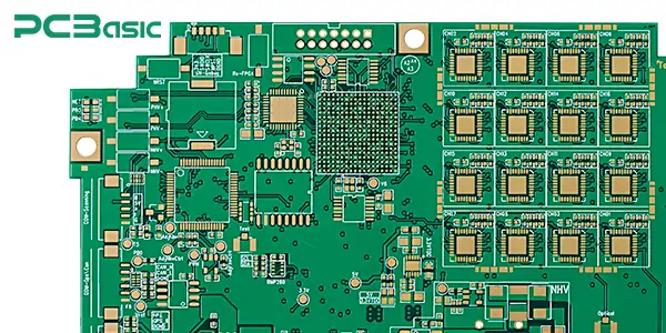
The structure of a double-sided PCB is more complex than that of a single-sided PCB. It has conductive copper layers on both sides, and the components can be installed on both sides. It uses via holes for the connection between signal layers, supporting a more compact PCB layout and a higher device density.
Multi-layer PCB
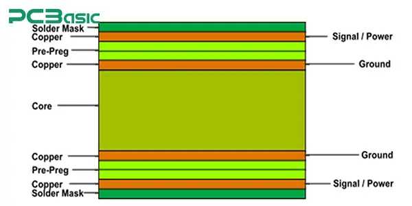
A multi-layer PCB is composed of three or more conductive layers stacked together. This type of PCB is widely used in products such as smartphones, laptops and medical devices. It supports high-density wiring and the implementation of complex functions. For high-speed PCB design and electromagnetic compatibility, multi-layer boards are the core structure.
From the perspective of mechanical structure, circuit boards can be classified into the following types:
Rigid PCB
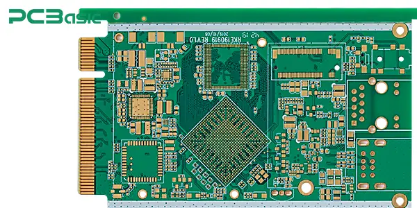
Rigid PCB is the most common type. It is made of hard materials such as FR-4 and cannot be bent. It is widely used in various traditional electronic boards. It is very suitable for beginners to learn the "parts of a circuit board" and the basic structure.
Flexible PCB
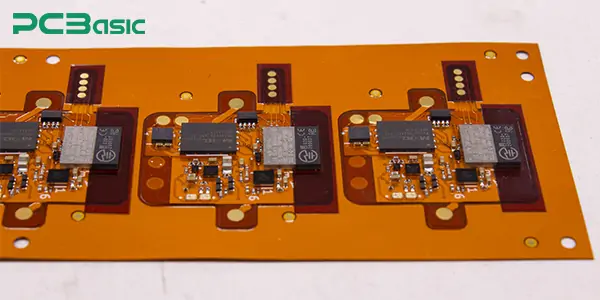
Flexible PCBs are made of polyimide or PET materials and can be bent and wound. It is often used in wearable devices, camera modules and other space-constrained occasions. Its design rules are different from those of rigid boards and it is a highly adaptable type of PCB.
Rigid-Flex PCB
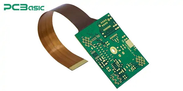
Rigid-flexible PCB is a hybrid PCB that combines rigid and flexible regions. This type of PCB is widely used in aerospace, military equipment and high-end consumer electronics. Compared with the traditional connection methods, this design can reduce connectors and improve the reliability of the system. It is a representative of advanced circuit board design.
Functional PCBs are customized to meet specific electrical performance or environmental requirements:
High-Frequency PCB
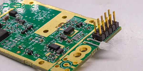
High-frequency PCBs are mainly used in RF communication systems. It can support GHz-level signal transmission and often uses special materials such as Rogers to ensure signal integrity.
Metal Core PCB
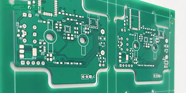
Metal-based PCB boards are embedded with metal cores (usually aluminum), which can enhance heat dissipation capacity. This type of PCB is widely used in the LED lighting field and is suitable for PCB components that have high requirements for thermal management.
HDI PCB
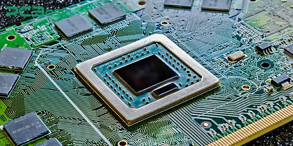
HDI PCBs adopt thinner traces, smaller hole diameters and a higher number of layers. Such circuit boards can achieve high-performance and compact designs and are commonly found in smartphones, tablet computers and industrial control devices.
RF PCB
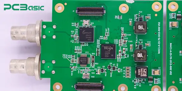
RF PCBs are often used in radars, satellites and advanced communication equipment. This type of PCB has extremely high requirements for materials and manufacturing precision.
In addition to the common types, there are also some specialized printed circuit boards for specific scenarios:
Aluminum-based PCB: It is a type of metal substrate and has good thermal conductivity. It is commonly used in LED drivers, power modules and other fields, and has a relatively low cost.
Ceramic PCB: It features excellent thermal conductivity and electrical insulation performance, and is suitable for high-voltage and high-frequency applications.
Transparent PCB: Made of acrylic or glass materials. It can transmit visible light and is often used in touch panels and some wearable electronic products.
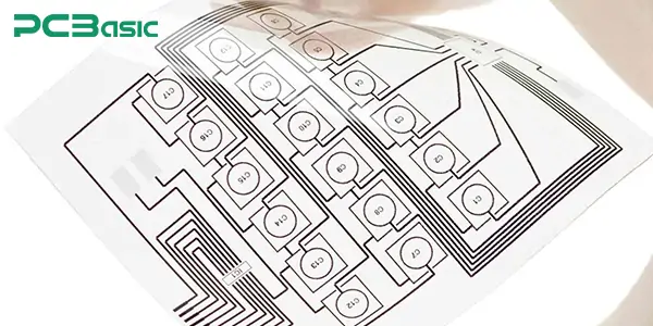
After understanding the types of circuit boards, the next equally important thing is to master their internal structure. A PCB is not merely a flat plate with copper wires - beneath its surface lies an elaborately designed multi-layer structure.
A standard PCB is usually composed of multiple key layers, and each layer has a specific function. These constitute the complete parts of a circuit board, including:

Substrate: The base layer of a PCB, typically made of FR-4 (glass fiber epoxy resin) material, providing mechanical strength and electrical insulation.
Copper Layer: One or more layers of copper located on top of the substrate, used to form electrical traces (i.e., lines/traces) and connect various PCB components.
Solder Mask: Commonly green (red, blue, black, etc.), is used to cover the copper layer and prevent short circuits during soldering circuit board basics, providing insulation and protection.
Silkscreen layer: Located on the top layer, it is used for printing component identifiers, logos, direction indicators, and other content.
In addition to the above core structures, many PCBs also contain vias, which are metal holes used to connect different copper layers. Common types of through holes include:
Through-hole Vias: Runs Through the entire circuit board, connecting the top layer and the bottom layer, and is widely used in SMT and THT circuits.
Blind Vias: It only connects the outer layer to a certain inner layer and does not run through the entire board.
Buried Vias: They exist only between the inner layers and are completely invisible from the outside.
A standard printed circuit board is mainly composed of the following materials:
The substrate is the framework of a PCB and also the basis for determining its mechanical strength and thermal stability. It is the support layer for all the circuit board parts. The main manufacturing materials of the base material are:
|
Material |
Key Features & Applications |
|
FR-4 |
Most common fiberglass epoxy. Good insulation, strength, and cost. Used in most consumer PCBs. |
|
Polyimide |
Flexible, heat-resistant. Ideal for flex PCBs in compact or bendable applications. |
|
PTFE (Teflon) |
Excellent high-frequency performance. Used in RF/microwave circuit board design. |
|
Ceramic |
High thermal conductivity and insulation. Used in high-power or industrial PCB components. |
|
Aluminum |
Great for heat dissipation. Common in LED and power applications. |
Copper is a key material for constituting circuit board components. It forms the traces of the circuit board and connects various parts of a circuit board. The thickness of copper (such as 1oz or 2oz) affects the current-carrying capacity and heat conduction efficiency, and is one of the core considerations in PCB layout design.
The dielectric constant (Dk) and loss factor (Df) will directly affect the signal transmission speed and integrity. Improper material selection may lead to signal interference and affect the stability and reliability of the entire circuit board design.
The following table shows some of the most common basic component types on PCBs:
|
Component |
Function & Usage |
|
Resistors |
Limit current and divide voltage. Fundamental in every electronic board. |
|
Capacitors |
Store and release energy. Used for filtering, coupling, and decoupling. |
|
Inductors |
Block AC and store energy. Common in power circuits and filters. |
|
Diodes |
Allow the current to flow in one direction. Used for rectification, protection. |
|
Transistors |
Amplify or switch electronic signals. Core building block in modern electronics. |
|
ICs (Integrated Circuits) |
Combine multiple functions into one chip. Central to PCB layout and design. |
|
Connectors |
Enable connections between the PCB and external devices or other boards. |
|
Switches, Buttons, LEDs |
Used for human interaction, status indication, and device control. |
Understanding the standard PCB design process is the first step towards professionalism. The design process of a circuit board is usually as follows:
Schematic design → Component selection → Components management → Layout and stacking planning → Wiring and line width calculation → Power supply and ground plane → Signal integrity consideration → Design rule check (DRC) → Generation of Gerber and drilling files
Learn more detailed: PCB Design Process
Below, we will introduce several commonly used PCB design tools and their applications to help you choose a platform that suits your project and skill level.
|
Software |
Target Users |
Key Features |
|
KiCad |
Beginners & Open-Source Users |
Free and open-source; supports schematics and PCB layout; great for education and light commercial use. |
|
Altium Designer |
Professional Engineers & Enterprises |
Industry-standard tool with powerful features, including schematics, simulation, and 3D view; a leading choice for advanced PCB design. |
|
Eagle (by Autodesk) |
Intermediate Designers |
Easy to learn, supports cloud collaboration; suitable for DIY and small-scale product development. |
|
EasyEDA |
Beginners & Online Designers |
Web-based, no installation required; includes a large component library and quick export/order options; ideal for learning what is a PCB board. |
|
OrCAD |
High-Speed & Professional Design |
Offers strong simulation and analysis features; ideal for complex system design and signal integrity verification in enterprise projects. |
When the PCB design and layout are completed, the next step is to transform the digital design into the actual physical circuit board. So, how to make a PCB? What is the manufacturing process of a finished product(PCBA) like?
The manufacturing processes of PCB and PCBA:
Cutting → Pattern transfer → Etching → Circuit inspection → Drilling → Electroplating → Solder mask → Silk-screen character printing → Surface treatment → Shape processing → Electrical testing → Full appearance inspection → warehousing
After the PCB manufacturing is completed, the bare board will enter the SMT PCB assembly stage. If multiple projects are involved in the production process, it is usually necessary to ensure the completeness of materials, check the BOM and issue work orders.
Learn more detailed: PCB Manufacturing Process
Pre-placement preparation → Solder paste printing → SPI → SMT placement → Reflow soldering → AOI inspection → Manual inspection/maintenance (if necessary)→ THT plug-in → Wave soldering → X-ray inspection → ICT Testing → FCT testing
Learn more detailed: PCB Assembly Process
After passing the functional test, the PCBA board will enter the subsequent processing stage.
Cleaning → Conformal coating (optional) → Panel separation (V-Cut/laser/stamping) → Final appearance inspection → Packaging → Shipment
In the manufacturing process of PCBs and PCBAs, there are many very important inspections and tests:
|
Test Type |
Process Stage |
What It Checks |
|
AOI |
After SMT / Reflow |
Solder defects, misalignment, missing parts, polarity errors, solder bridges |
|
X-ray Inspection |
For BGA, QFN, hidden joints |
Voids, bridging, cold solder joints, misaligned solder balls |
|
ICT |
After PCBA |
Resistance, capacitance, voltage levels, short/open circuits, diode polarity |
|
FCT |
After ICT / Final testing |
Verifies actual circuit function: power output, communication, response, display |
|
Flying Probe Test |
After PCB fabrication |
Checks for shorts, opens, and continuity errors in PCB layout |
|
Visual & Manual Inspection |
After assembly & soldering |
Solder joints, silk errors, dirt, tilted or misplaced components |
|
Cleaning & Conformal Coating Check |
Post-assembly / Final stage |
Residue removal, coating coverage, protection against moisture & dust |
Printed circuit boards, with their diversity, scalability and high reliability, are widely used in electronic products across various industries. Some examples are listed below:
In the field of consumer electronics, PCBs are widely used in smartphones, laptops, tablets, televisions, game consoles and wearable devices, etc. This type of product usually requires a compact PCB size and has high requirements for the wiring density and signal integrity of the circuit board design.
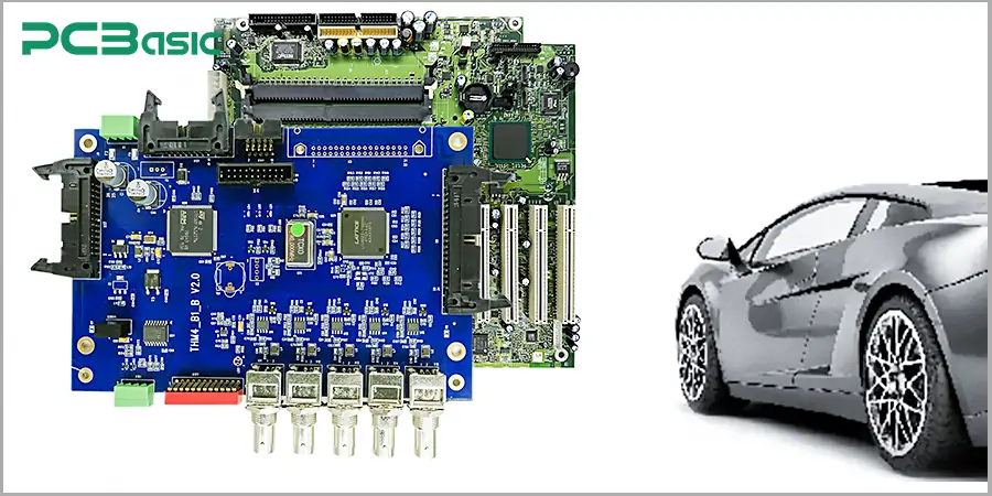
The automotive industry is highly dependent on PCBs for engine control units (ECUs), infotainment systems, lighting modules, battery management systems (BMS), and advanced driver assistance systems (ADAS). These application environments are harsh, and extremely high requirements are placed on the heat resistance, shock resistance and stability of the electronic board.
In industrial equipment, PCBs are used in motor controllers, programmable logic controllers (PLCS), sensors, robots and automation systems. This type of application places higher demands on the durability, heat dissipation performance and long-term stability of PCB components.
Medical electronics is also an important field for PCB applications. Medical PCBs need to meet strict quality standards such as ISO 13485. So, what other standards are there for the manufacturing of PCBs and PCBA? Let's take a look below.
|
Standard / Certification |
Scope |
Description / Purpose |
|
IPC-A-600 |
PCB manufacturing quality |
Defines acceptance criteria for the physical characteristics of printed circuit boards |
|
IPC-A-610 |
PCBA assembly quality |
Specifies acceptance criteria for soldering circuit board basics and component placement |
|
IPC-2221 |
General PCB design |
Generic standard for PCB design rules and layout practices |
|
IPC-7351 |
SMT footprint design |
Guidelines for PCB layout and land pattern dimensions for surface-mount components |
|
ISO 9001 |
Quality management systems |
International standard for consistent quality across production and services |
|
ISO 13485 |
Medical device manufacturing |
Quality management standard specific to medical electronic boards |
|
IATF 16949 |
Automotive electronics |
Global quality standard for automotive-grade PCB components and systems |
|
RoHS |
Environmental compliance |
Restricts use of hazardous substances in electronics (e.g., lead, mercury, cadmium) |
|
REACH |
Chemical safety |
Regulates chemical substances used in PCB materials |
|
UL Certification |
Product safety (flammability) |
Ensures PCB boards meet flammability and electrical safety standards |
|
CE Marking |
EU compliance |
Required for selling finished electronic products in the European market |
This article systematically introduces the types, structures, common materials, production processes, industry standards and typical applications of printed circuit boards. These contents together constitute the core of "printed circuit board basics" and can help you build a clear bridge from conception to the actual product.
Time is money in your projects – and PCBasic gets it. PCBasic is a PCB assembly company that delivers fast, flawless results every time. Our comprehensive PCB assembly services include expert engineering support at every step, ensuring top quality in every board. As a leading PCB assembly manufacturer, we provide a one-stop solution that streamlines your supply chain. Partner with our advanced PCB prototype factory for quick turnarounds and superior results you can trust.
 About PCBasic
Assembly Enquiry
Instant Quote
Phone contact

+86-755-27218592
In addition, we've prepared a Help Center. We recommend checking it before reaching out, as your question and its answer may already be clearly explained there.
Wechat Support

In addition, we've prepared a Help Center. We recommend checking it before reaching out, as your question and its answer may already be clearly explained there.
WhatsApp Support

In addition, we've prepared a Help Center. We recommend checking it before reaching out, as your question and its answer may already be clearly explained there.