
Global high-mix volume high-speed PCBA manufacturer
9:00 -18:00, Mon. - Fri. (GMT+8)
9:00 -12:00, Sat. (GMT+8)
(Except Chinese public holidays)





HomePage > Blog > Knowledge Base > Wireless Communication PCBA: From RF Design to Assembly and Testing
Table of Contents
1. What Is a Wireless Communication PCBA?
2. Key Design Considerations for Wireless and RF PCBAs
3. Wireless PCB Assembly Process
4. Testing and Manufacturing Challenges in Wireless Communication PCBA
In wireless PCB construction, this is also the most challenging step. The product can sometimes show weak signals, shorter communication distances, and inconsistent reception even when the solder connections appear OK and AOI can pass normally. RF performance can be influenced by PCB layout, antenna positioning, shielding, grounding, component choice, and soldering quality.
Therefore, we should not only focus on whether SMT is completed successfully in wireless communication PCB assembly; it also needs to consider the design, RF PCB assembly, and testing together. This article will mainly introduce the key factors that affect the quality of wireless communication PCBA in these aspects.
A circuit board that has completed the component assembly and is capable of wireless signal transmission, reception, and data processing is known as a wireless communication PCBA. Its purpose, to put it simply, is to allow devices to interact without the need for physical cable connections. Products that use wireless technologies like Wi-Fi, Bluetooth, Zigbee, LoRa, cellular, GPS/GNSS, NFC, etc. frequently use it. Wireless communication, power supply, control, and data processing circuits must all be integrated into the same board, even though various products employ different communication protocols.
A typical wireless communication PCBA usually consists of:
• MCU or processor: runs programs and processes data
• RF transceiver: transmits and receives wireless signals
• Power management circuit: provides stable voltage for different chips
• Filter, amplifier and matching components: help improve RF signal quality
• Crystal or oscillator: provides a stable clock signal
• Antenna, antenna connector or wireless communication module
• Shielding can: help reduce external interference and interference between circuits
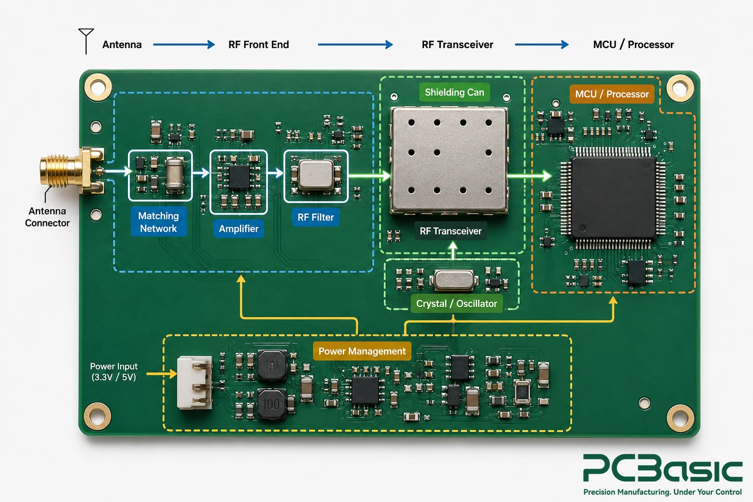
Wireless PCB forms the basis for the operation of these components. In RF, signal performance is affected by things like trace length, impedance, grounding, vias and antenna location. The RF PCB, RF circuit board or high-frequency PCB can be used for the products with higher frequency or higher signal loss requirements with corresponding materials and stack-up structure.
In RF PCB assembly, component placement, soldering quality, shielding structure and manufacturing tolerances also influence the final wireless performance. These kind of PCBA are widely used in IoT devices, smart home, industrial control, wireless gateways, communication equipment, automotive electronics and positioning devices. Different communication PCB assemblies will also vary in design and manufacturing because of different communication ranges, power consumption and data rate requirements.
A stable wireless communication PCBA cannot be evaluated solely based on the wireless module. PCB traces, grounding, antenna placement, component layout, power design and materials all affect RF performance. These designs also influence the smoothness of subsequent assembly, testing and inspection.
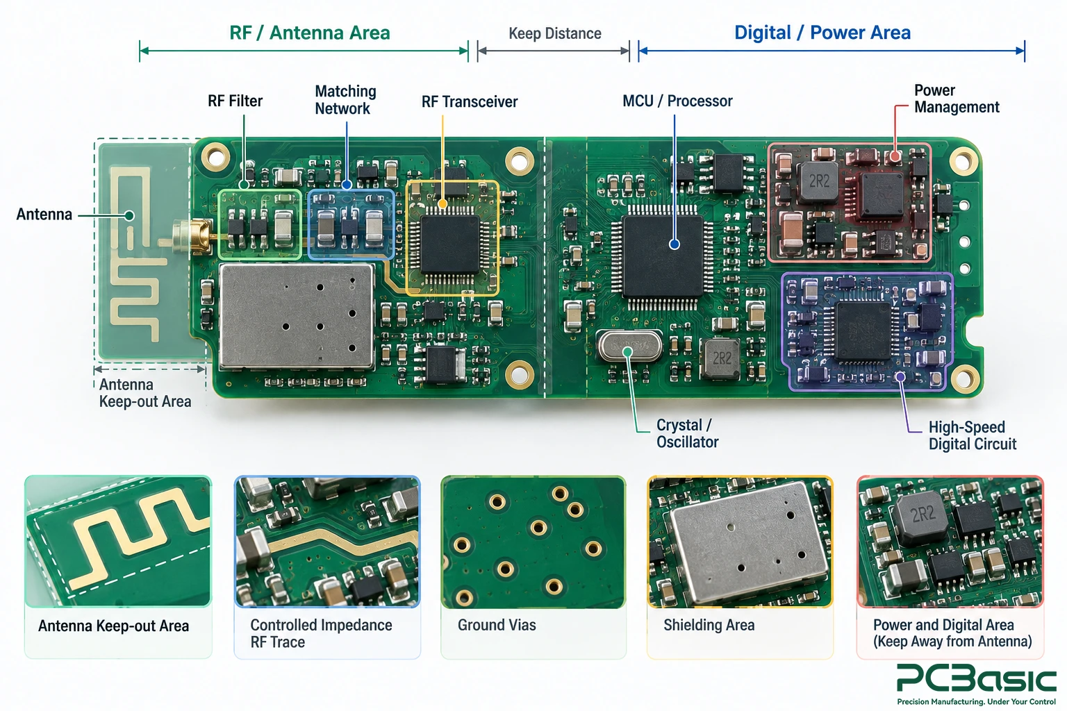
In RF PCB or high frequency PCB, RF traces require stricter control than ordinary signal lines. Trace width, dielectric thickness, vias, layer changes and reference planes all affect impedance and signal loss.
Keep the RF key paths as short as possible and the reference ground should be continuous. It is also important to reduce unnecessary vias and abrupt changes in trace size or structure. These details are equally important in RF PCBA production, as small deviations in PCB manufacturing or assembly can impact the final RF performance.
The placement of the antenna directly affects wireless performance. The antenna should be as far away as possible from switch power supplies, high-speed clocks and other strong interference sources. If using PCB antennas or module antennas, corresponding clearance areas should be reserved as required.
Component placement is also important. Matching capacitors and inductors should be placed as close as possible to the corresponding RF paths; decoupling capacitors should be placed close to the power pins. Sensitive RF areas should also be separated from noisy digital circuits or power circuits.
For wireless communication PCBA, the enclosure and nearby metal structures should also be considered, as these factors may also affect the actual performance of the antenna.
You don’t need to use expensive high-frequency materials for all wireless products. Some designs are able to meet requirements with the right type of FR-4, but applications with higher frequencies or tighter signal loss requirements may require specialized high frequency materials.
The choice of the material should be based on the operating frequency, loss requirements, stack-up, cost and manufacturing capability.
In the design stage, manufacturability should also be considered. For high frequency PCB assembly, sufficient space should be reserved for solder paste printing, SMT assembly, testing, shield installation and repair.
A good design not only ensures that the first prototype works properly, but also enables stable replication in wireless PCB assembly, RF PCB assembly and subsequent batch production.
Wireless PCB assembly does not start with the pick-and-place machine; instead, it begins with pre-production review. Before production, manufacturers usually check Gerber files, BOM, placement data, PCB layers, impedance requirements, stencil design, component polarity, packaging form, and shielding requirements.
For wireless communication PCB assembly, RF-related components also require additional verification. Especially for matching networks, filters, and other high-frequency components, even if the nominal parameters of the substitutes are the same, their actual RF performance may differ. Therefore, one cannot simply rely on the model or numerical values.

After production begins, the solder paste is first printed onto the pads through the screen, and then SPI is used to check the height, area, and position of the solder paste. For fine-pitch ICs, small passive components, QFN, BGA, LGA, and wireless modules, a stable amount of solder paste is very important.
During SMT placement, component type, orientation, and position of the components need to be controlled well. In RF PCBA and high-frequency PCB assembly, very small capacitors and inductors are often used, and they may directly participate in impedance matching or filtering, so positional deviations not only affect soldering but also may affect RF performance.
If moisture-sensitive components are used, storage, baking, or other handled should be done according to the component grade.
After placement, the PCB enters the reflow soldering furnace. The temperature curve needs to be set according to the PCB structure, solder, and component requirements, ensuring that the solder joints are fully formed while avoiding excessive thermal stress on the components or the PCB.
After reflow, AOI mainly checks the position, polarity, and visible solder joints of the components. For BGA, QFN, LGA, and some hidden solder joints at the bottom of wireless modules, X-ray can be used for further inspection.
RF PCB assembly may also include secondary processes such as RF connectors, shielding covers, through-hole components, hand soldering, or cleaning, depending on the product structure.
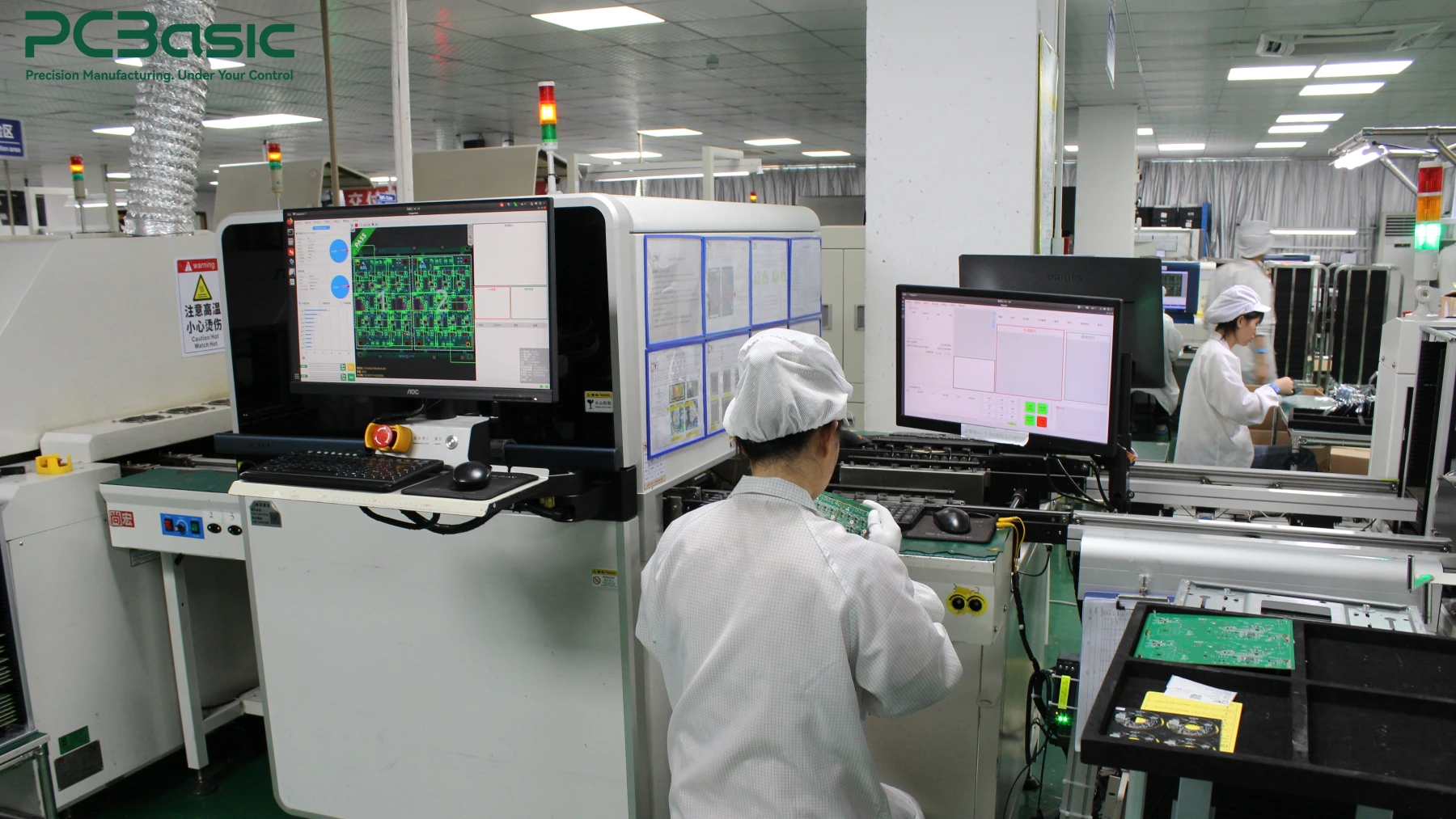
Wireless PCBAs cannot be judged solely by "whether the soldering is correct". Electrical testing and functional testing also need to confirm whether the board can be powered on, communicate, and operate normally. Some products may also need to test pairing, signal transmission and reception, connection stability, or other RF functions.
A typical process may look like this:
DFM review → Material confirmation → Solder paste printing → SPI → SMT placement → Reflow soldering → AOI/X-ray → Secondary assembly → Electrical and functional testing
For telecommunication PCB assembly, it is also important to retain material batches, process parameters, inspection records, and test results. In case of abnormalities, these data can help locate the problem more quickly and ensure the consistency of subsequent batch production.
Wireless communication PCBA cannot be judged as qualified solely by AOI or X-Ray inspection. These tests can detect component misalignment, soldering defects, and hidden solder joints, but they cannot directly prove the stability of wireless communication.
According to product requirements, flying probe testing, ICT, or functional testing can be used to check open circuits, short circuits, power rails, interfaces, and basic functions. For RF PCBA, further tests may also be necessary:
• Whether the pairing and connection are normal
• Whether the signal transmission and reception are stable
• Output power and receiving sensitivity
• Frequency and communication stability
The test requirements for different products are not the same. For Bluetooth sensors, Wi-Fi controllers, and high-performance RF devices, the same communication PCB assembly testing scheme should not be used. Therefore, wireless function testing is usually an important step in wireless PCB assembly.
Wireless products are also prone to be affected by component substitution, shield can installation, RF connector soldering, solder-volume variation, and impedance deviation during production.
For example, even if two capacitors have the same nominal value, their actual characteristics at high frequencies may be different. If they are used in an RF matching network, it may change the final performance. Similarly, if the stack-up or impedance of the RF circuit board deviates from the design requirements, even if the RF PCB assembly itself has no obvious problems, the wireless performance may still be affected.
For this reason, a stable wireless communication PCB assembly requires considering PCB fabrication, assembly, testing, and RF function testing together. The ultimate goal is not just to make the circuit board pass the inspection, but to ensure consistent wireless performance from the prototype to mass production.

Wireless communication PCBA project usually has higher requirements than standard PCBA projects, because even minor changes in the design or production process can affect the wireless performance of the product in actual use. The key is to make sure that design, assembly, inspection and testing work together smoothly rather than as separate steps.
PCBasic can support wireless PCB assembly from prototype to mass production, including DFM review, component sourcing, SMT/DIP assembly, AOI, X-Ray inspection, flying probe testing, ICT, functional testing and final assembly. This reduces the manufacturing risks for the customer and enables more stable production at higher production volumes.
If you are developing RF, IoT, wireless or communication products, you can contact PCBasic to discuss your PCBA requirements and testing specifications further.
Q1: What is the difference between an RF PCB and an RF PCBA?
A1: An RF PCB is the bare board designed for radio-frequency signals, while an RF PCBA is the finished board with components mounted and soldered. RF PCB assembly adds RF ICs, filters, matching components, connectors, shielding, and other required parts.
Q2: Does every wireless communication PCBA need high-frequency PCB material?
A2: No. Some wireless PCB designs can use suitable FR-4. Special low-loss materials are usually needed only when frequency, signal loss, impedance, or performance requirements are more demanding.
Q3: How is wireless PCB assembly tested?
A3: Wireless PCB assembly may use AOI and X-ray for inspection, flying probe or ICT for electrical checks, and functional testing for communication and interfaces. Depending on the product, wireless communication PCBA may also require RF tests for signal strength, connectivity, or receiver performance.

Assembly Enquiry
Instant Quote


Phone contact

+86-755-27218592
In addition, we've prepared a Help Center. We recommend checking it before reaching out, as your question and its answer may already be clearly explained there.
Wechat Support

In addition, we've prepared a Help Center. We recommend checking it before reaching out, as your question and its answer may already be clearly explained there.
WhatsApp Support

In addition, we've prepared a Help Center. We recommend checking it before reaching out, as your question and its answer may already be clearly explained there.
