
Global high-mix volume high-speed PCBA manufacturer
9:00 -18:00, Mon. - Fri. (GMT+8)
9:00 -12:00, Sat. (GMT+8)
(Except Chinese public holidays)





HomePage > Blog > Knowledge Base > PCB Component Placement Guidelines: How Placement Affects Routing, Assembly, and Reliability
Table of Contents
1. What Is Component Placement in PCB Design?
2. How to Start PCB Component Placement
3. Electrical and Thermal Factors in Component Placement
4. PCB Component Placement for Manufacturing and Assembly
5. Designing for Testing, Inspection, and Accessibility
Therefore, a reasonable component placement needs to take into account both electrical, mechanical, thermal, and manufacturing requirements. The actual PCB layout rules should not only consider the spacing between components, but also make the subsequent routing easier and leave appropriate room for assembly, inspection, testing, and rework.
In this article, we will introduce the layout principles that need to be focused on in actual PCB design from several aspects: the basic concept of PCB component placement, the initial layout steps, electrical and thermal design, manufacturing and assembly requirements, as well as testing and accessibility.
The process of deciding where and how to organize electronic components on a printed circuit board is known as PCB component placement. It may be summed up as converting the circuit connection relationships in the schematic into the actual physical layout on the board for those who are looking for "what is PCB place"?
A proper PCB component placement takes into account signal flow, heat dissipation, available board space, routing, assembly, and mechanical construction constraints all at once. Related components are often put as close together as feasible, resulting in shorter and more direct traces; however, components with high noise, high speed operation, or high heat generation may necessitate particular spacing or separation considerations. Appropriate component placement can reduce the number of needless vias and complex traces, improve signal and thermal performance, and simplify PCB manufacturing and assembly.
A good PCB component placement process should start with the parts that have the least flexibility in position. Instead of placing the components one by one, it is better to determine the overall mechanical structure and functional divisions of the circuit board first. A practical placement order is as follows:
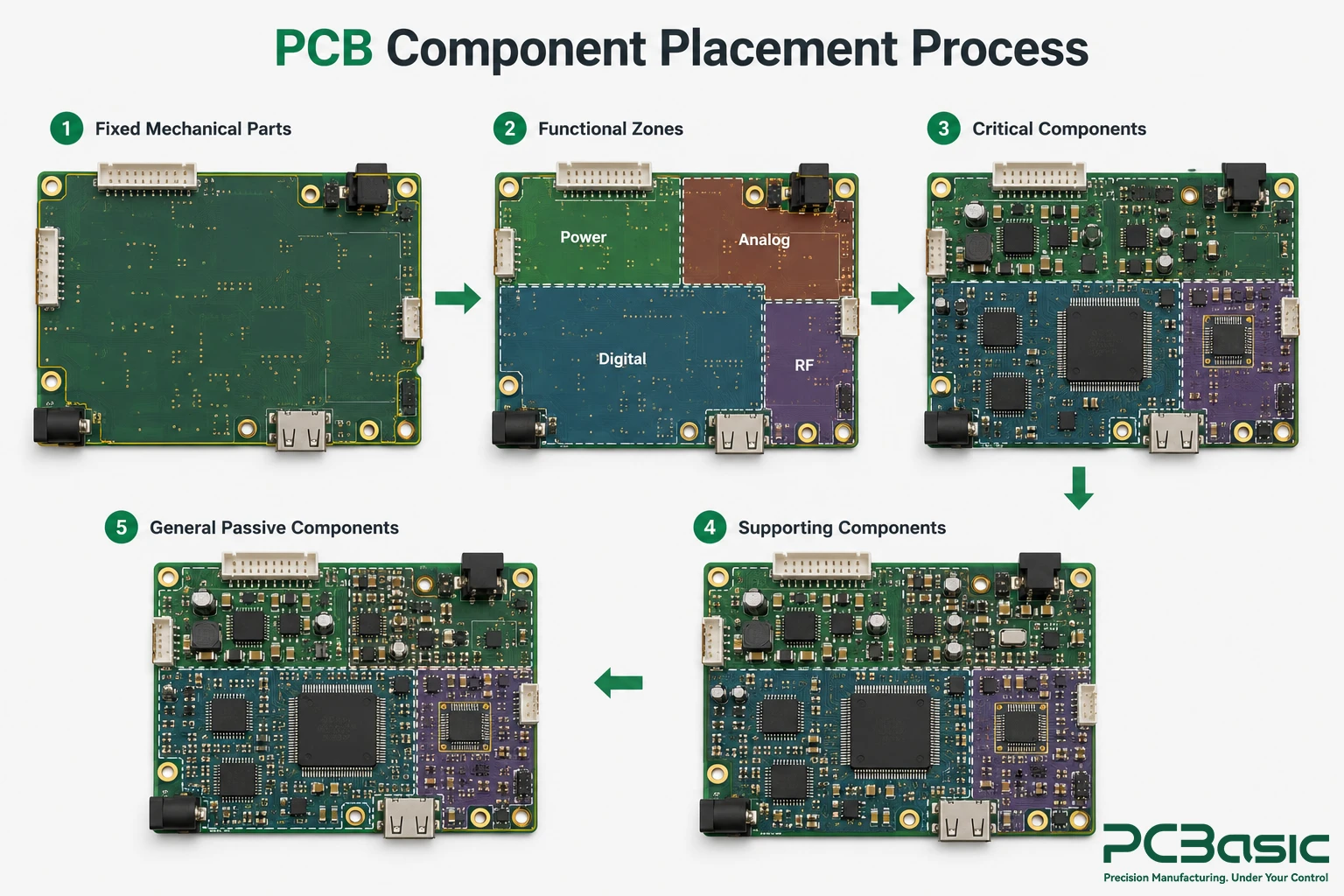
First, determine the board outline, mounting holes, connectors, switches, antennas, prohibited areas, and other mechanical restrictions. These positions are usually determined by the enclosure, interface locations, or product structure, so they should be fixed before arranging other components.
You can divide it according to functions such as power, analog, digital, RF, sensors, communication, or control sections. This is one of the very practical PCB layout rules, as it helps to keep noisy circuits away from sensitive circuits. For example, if conditions permit, high-current or high-frequency areas should be kept at a certain distance from low-level analog circuits and sensor circuits.
Processors, FPGAs, memory devices, regulators, transformers, power devices, and other major ICs usually have the greatest impact on subsequent routing and circuit performance. Therefore, the positions of these components should be determined first before smaller and more flexible parts.
According to the actual electrical function, place the critical capacitors, resistors, filters, and other supporting components near the devices they serve.
General resistors, capacitors, and other passive components with relatively flexible positions can be arranged after the main layout structure of the circuit board is determined.
By following this sequence for PCB component placement, the entire layout can be made clearer from the very beginning, and it also helps to reduce subsequent routing conflicts, noise coupling, and unnecessary layout modifications later in the design.

When performing component placement, electrical performance and thermal management usually need to be considered together. It is difficult to focus only on one aspect because where the components are placed often simultaneously affects the routing, signal quality, and heat dissipation.
If the distance between critical components is too far, the design may require longer routing, more vias, and more complex signal paths later; if the heat-generating components are concentrated in the same area, local hotspots may form. Therefore, addressing these issues during the layout stage is usually more effective than relying on routing or thermal measures for remediation later.
When working on signal-related PCB component placement, we can first look at the relationships between components along the signal flow. For example, a signal enters the PCB from a connector, passes through protection and filtering circuits, then enters the interface IC, and finally reaches the processor. It is best to arrange the layout in this order as well. The benefits are clear: shorter routing, no need for repeated loops, and easier handling of subsequent routing.
In actual PCB design, you can focus on checking these PCB layout rules:
• Place high-speed devices such as processors, memory, oscillators, and other devices close to the components they are directly connected to.
• Clock lines, differential pairs, and other critical connections should be kept short and direct.
• Try to minimize unnecessary signal backtracking, crossings, and excessive vias.
• Sensitive analog signals and low-level signals should be kept away from high-current and high-speed switching areas.
• Keep the high-speed signals below a continuous reference plane to avoid crossing or splitting the plane at will.
• Decoupling capacitors should be placed as close as possible to the corresponding power pins, rather than randomly placing them after leaving the remaining empty space.
If you notice that a critical network needs to be routed over a long distance or requires continuous increases in vias during the initial routing, you may not necessarily rush to "optimize the routing". In many cases, it is better to first check the PCB component placement and adjust the positions of relevant components more reasonably, making the problem easier to solve.
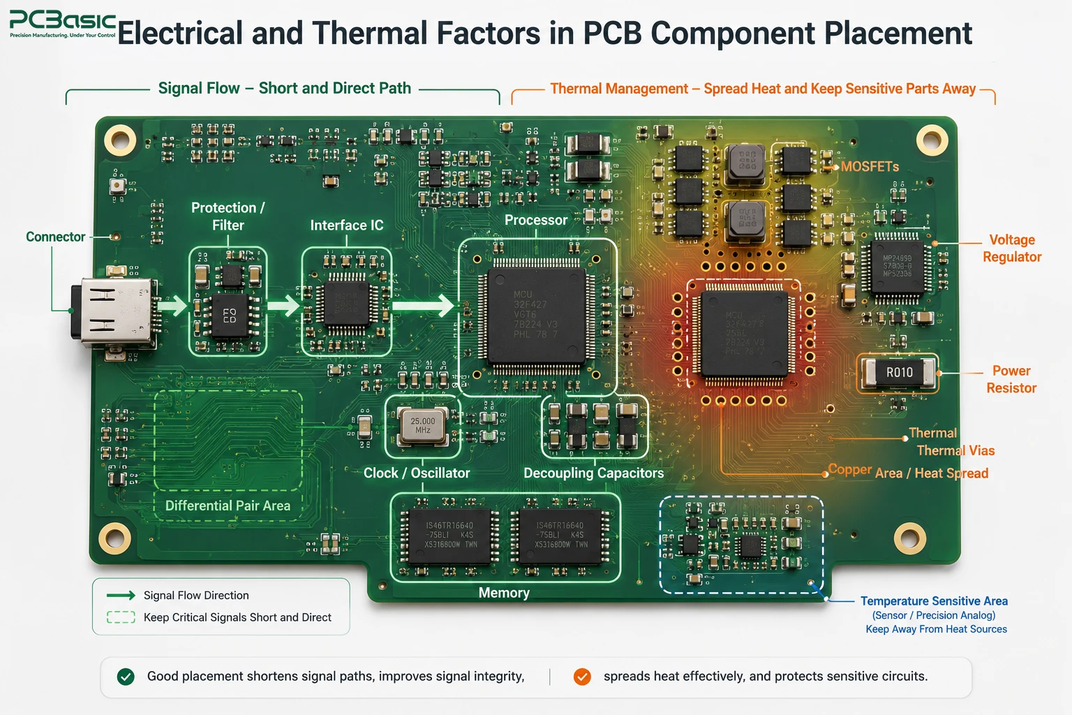
Thermal management is also a part of component placement that is often underestimated. Devices such as processors, MOSFETs, voltage regulators, and power resistors generate heat when they operate. If they are concentrated in a small area, even if the temperature of a single device seems acceptable, the entire area may gradually form a hot spot.
When planning the PCB component placement, we usually also consider the following issues:
• Are high-power devices too concentrated and is it necessary to appropriately disperse them?
• Is the position of the heat-generating devices convenient for using air flow, heat sinks, thermal vias, or large copper foils?
• Are temperature-sensitive components such as sensors and precision analog devices too close to the main heat source?
• Are tall components blocking fans or main air flow paths?
The focus here is not simply to separate all heat-generating devices. What matters is where the heat ultimately goes. A reasonable component placement for thermal management should leave a clear heat dissipation path for the main heat source and keep temperature-sensitive devices away from obvious heat-affected areas.
Even if a PCB has no electrical design issues, if the component placement does not align with the actual manufacturing process, problems may still arise during the assembly stage. Therefore, before finalizing the layout, we usually need to recheck it from a manufacturing perspective: how the board will be soldered, inspected, and disassembled, and whether it is convenient for rework in case of problems.
Some practical PCB layout rules include:
• Ensure there is an appropriate spacing between components.
If they are placed too closely together, although it may save board space, soldering, AOI inspection, and later rework will be more difficult. The exact amount of space needed depends on the package size, assembly method, detection method, and the manufacturing capabilities of the PCB assembly factory.
• Pay attention to the board edges and the disassembly area.
If the components are too close to the routed edge, V-Cut, or breakaway areas, mechanical stress generated during disassembly and handling may affect the solder joints or the components themselves. Therefore, these areas usually need to be reserved with safety space in advance.
• Arrange the component placement and orientation reasonably.
Direction-sensitive components such as diodes, LEDs, polarized capacitors, and ICs should have their polarity or Pin 1 clearly marked for easy identification. For the same type of components, if conditions permit, they can be kept in the same orientation. However, if this affects routing or thermal performance, it is not necessary to forcibly unify them for the sake of "looking neat".
• The layout should be coordinated with the actual soldering process.
The requirements for component positions and spacings vary for different assembly methods such as SMT reflow soldering, wave soldering, selective soldering, and manual assembly. For example, when using wave soldering, we also need to pay attention to the component orientation, height, and whether large components will block the subsequent welding area.
• Don't forget to leave space for repair.
During actual repair, technicians may need probes, tweezers, soldering irons, or hot air guns. If the components are blocked by large components or there is almost no operation space around, subsequent maintenance and rework will become very troublesome.
In fact, there is no fixed set of spacing or component placement and orientation rules that works for all PCBs. A more reliable approach is to review the PCB component placement before production by combining actual DFM and assembly requirements. This can help detect problems in soldering, testing, and rework earlier and reduce the need to re-modify the layout for production purposes later.
PCB component placement cannot only consider whether the circuit board can be assembled. After the PCBA is produced and rolled off the production line, it usually needs to undergo electrical testing, inspection, programming, debugging, and sometimes even rework. All these processes require actual operations on the relevant positions on the circuit board.
For ICT or flying probe testing, the test points need to be placed at positions where the fixtures or probes can actually come into contact. Even if a test point is correctly connected in the CAD file, if it is located beneath a large-sized device or too close to a tall connector, it may still be difficult to use during actual testing.
The appropriate spacing between test points, between test points and components, and between test points and the edge of the board will vary depending on the testing method and the equipment used by the manufacturer. Therefore, test accessibility should be considered in advance during the PCB component placement stage, rather than being added after the routing is completed.
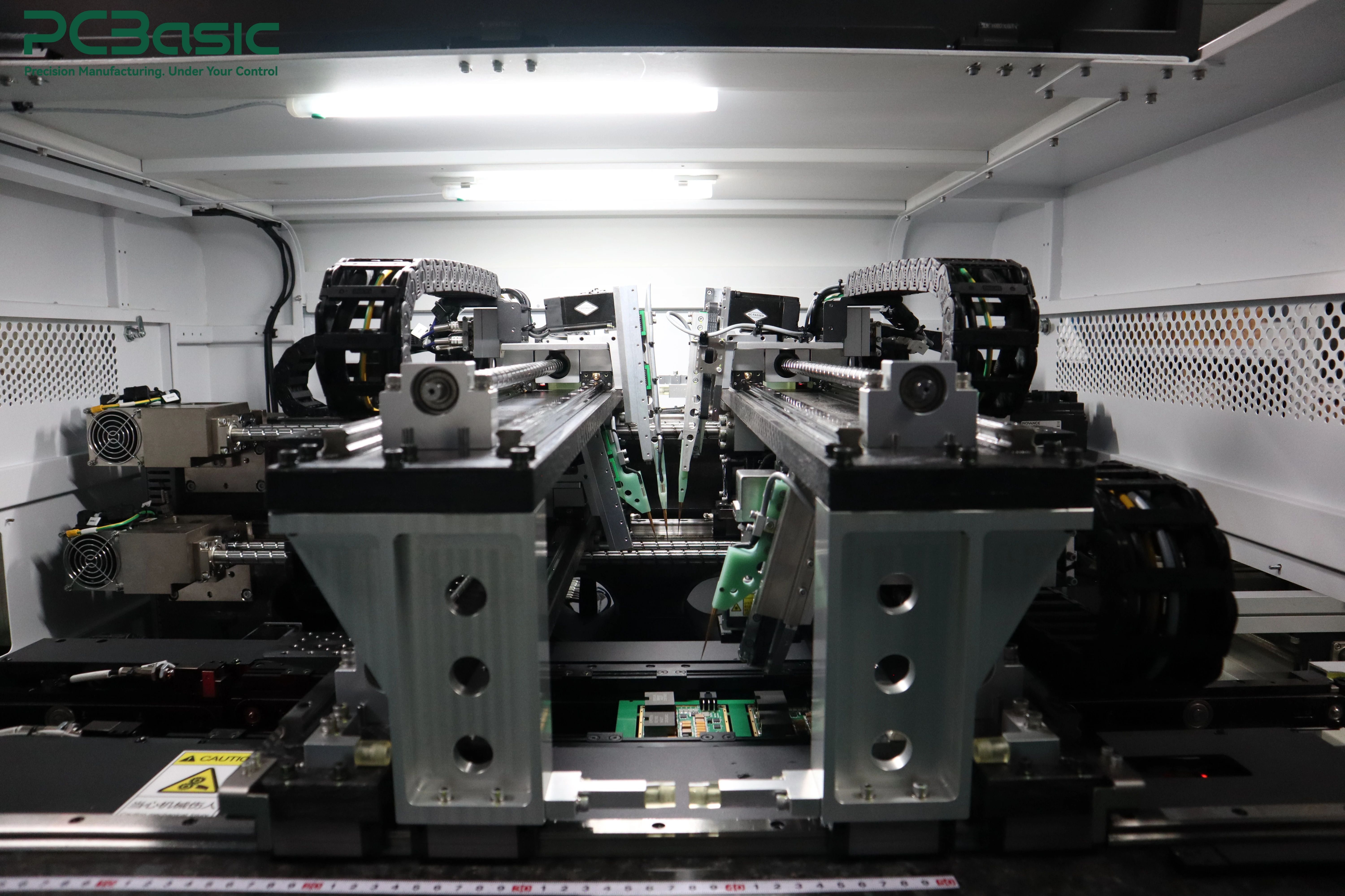
The arrangement of components also affects the inspection results. If the components are placed too closely together, whether using AOI or manual inspection, the difficulty will be much greater. For BGA packages where the solder joints are hidden at the bottom of the components, X-ray inspection may also be necessary.
Rework is the same. If certain components may need replacement, debugging, or undergo engineering modifications in the future, it is best to leave sufficient space around them so that probes, tweezers, soldering irons, or hot air tools can operate normally. This is especially important for prototype and NPI builds, as such projects are more prone to modification requirements.
Judging the accessibility cannot only rely on the bare PCB. It should also be considered in conjunction with the final assembly state of the product. For example, parts like programming interfaces and connectors, which seem to have ample operating space in the PCB design software, may be blocked by heat sinks, enclosures, cables or another circuit board after installation, making it impossible to operate normally.
Panelization also affects the component placement. If the components are too close to V-Cuts, broken connection points or routed edges, they are prone to mechanical stress during splitting. Leaving sufficient spacing in these areas in advance can better protect the components and solder joints.
In simple terms, PCB component placement not only needs to make the circuit board easy to assemble, but also needs to make subsequent testing, inspection, debugging and maintenance more convenient.

A proper PCB component placement aims not to make the layout look neater, but to facilitate the smooth progress of the design into the manufacturing, assembly and testing stages. Many problems that only surface later can actually be identified and adjusted during the placement stage.
This is why in actual projects, PCB layout rules should not only be limited to the CAD design level, but also need to be checked in conjunction with the actual production capacity. PCBasic can conduct DFM reviews for component spacing, board edge areas, welding methods, test points and manufacturability according to PCB manufacturing and PCBA assembly requirements before the project goes into production, and provide services such as PCB manufacturing, component procurement, SMT/DIP assembly, AOI, X-ray, flying probe testing and functional testing.
If your design is ready complete, you can submit your Gerber files, BOM and assembly files to PCBasic, allowing the PCBasic engineering team to help check potential manufacturing and assembly issues before production.
Q1: What does what is PCB place mean?
A1: The search phrase what is PCB place generally refers to what PCB placement is. In PCB design, placement means arranging component footprints on the board before detailed routing so that electrical, mechanical, and manufacturing requirements can be met.
Q2: Which components should be placed first on a PCB?
A2: Start PCB component placement with mechanically constrained parts such as connectors, switches, mounting holes, antennas, and external interfaces. Then establish functional zones and position major ICs, power devices, and other critical components before general passive parts.
Q3: How does component placement affect PCB routing?
A3: Good component placement can shorten critical connections, reduce routing crossings and unnecessary vias, simplify differential-pair and power routing, and provide more direct signal paths. Poor placement often forces traces to take longer and more complicated routes.

Assembly Enquiry
Instant Quote





Phone contact

+86-755-27218592
In addition, we've prepared a Help Center. We recommend checking it before reaching out, as your question and its answer may already be clearly explained there.
Wechat Support

In addition, we've prepared a Help Center. We recommend checking it before reaching out, as your question and its answer may already be clearly explained there.
WhatsApp Support

In addition, we've prepared a Help Center. We recommend checking it before reaching out, as your question and its answer may already be clearly explained there.
