
Global high-mix volume high-speed PCBA manufacturer
9:00 -18:00, Mon. - Fri. (GMT+8)
9:00 -12:00, Sat. (GMT+8)
(Except Chinese public holidays)





HomePage > Blog > Knowledge Base > PCBA Manufacturing Challenges: What to Check Before the First Build
Table of Contents
1. Which Part Shortage Becomes a Wrong Part on the Board?
2. What Should the Engineering Review Catch Before the Stencil Is Cut?
3. Which Solder Defects Can the Line Catch?
4. What Record Shows the Build Was Tested?
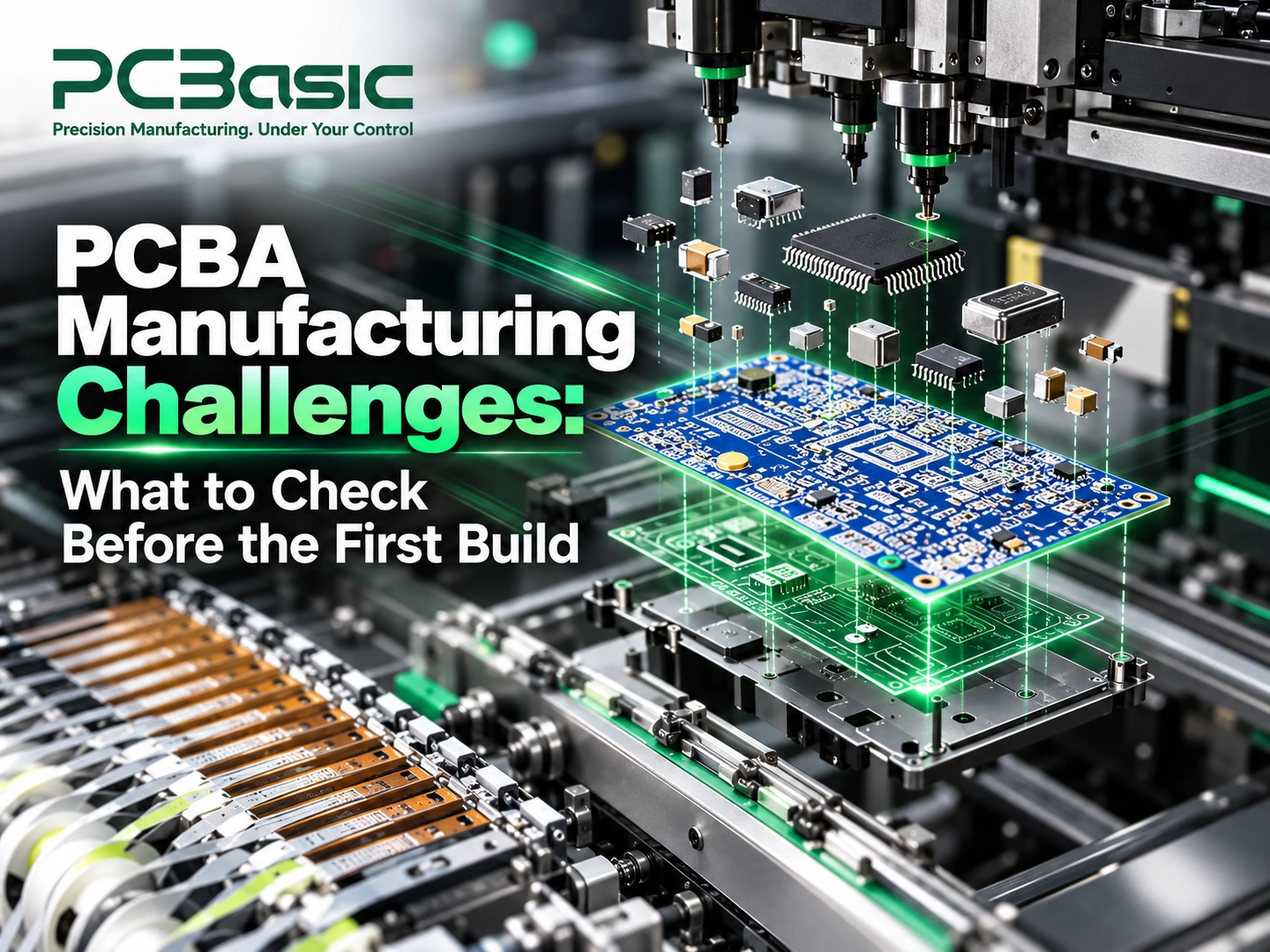
PCBA manufacturing challenges show up in a familiar way. The sample works on your bench. The next build does not.
The cause is usually one of four things. The part is wrong or missing. The design files do not match. The solder joint is bad. The test was never written down.
The table below is the checklist for the four problems. Each section takes one row. It says what to send, and what record to ask for.

A late part delays the build. A wrong part goes onto the board. Watch for a component package that does not match the PCB footprint, or a substitute that nobody approved.
The mistake happens between two steps of the PCBA process. One person buys the part. Another person places it. When two companies split those steps, the assembler sees the wrong package only when the carton arrives.
We buy parts from the original manufacturers and from authorized first-tier distributors. Common parts are kept in stock, so a small build does not have to take a full reel. Incoming lots go through IQC (incoming inspection). Before the parts are loaded for placement, we check the BOM (the parts list) against the parts that arrived.
Mark which lines on the parts list may use an alternate, and which lines may not. Ask to see any substitute before it is placed. Ask for the incoming inspection record.
Some problems are already in the files. Solder inspection will not remove them.
Pads that are not the same size can increase the risk of a small part lifting onto one end. A board with no accessible test points can limit fixture access later. A Rev C board built from a Rev B parts list can fail even when every joint looks right.
The stencil is the metal sheet used to print the solder paste. After it is cut, a change to its openings may require a new stencil. A change to the PCB pads requires updated board files and, if the bare boards have already been made, usually new boards.
In our flow, process evaluation comes before the stencil is made. We can send written comments on the design and the process. The review reads the Gerber files, the BOM, and the pick-and-place file together. The Gerber files are the board artwork. The pick-and-place file tells the machine where each part goes.
Send the Gerber and drill files, a BOM with manufacturer part numbers, the pick-and-place file, and an assembly drawing that marks pin 1 and which way each part faces. Ask which items need a change before the stencil is ordered.
Two common solder defects are easy to see once you know the names.
A bridge is solder that joins two conductors that should stay separate. A tombstone is a small part that stands up on one end, so the other end is not soldered. A BGA (ball grid array) package has its solder joints hidden under the body. A camera looking down cannot see those balls.
Bridges and tombstones often start in the paste or in the pad design. Too much paste can contribute to bridging. Uneven paste deposits, unequal pads, or uneven heating can contribute to tombstoning. The file review above is where those pad design problems should be caught. A BGA can look fine from above and still have an open joint underneath.
SPI (solder paste inspection) measures the solder paste before the parts are placed. After the board is soldered, AOI (automated optical inspection) uses a camera to check visible solder features. We also have X-ray for joints the camera cannot see, such as the balls under a BGA.
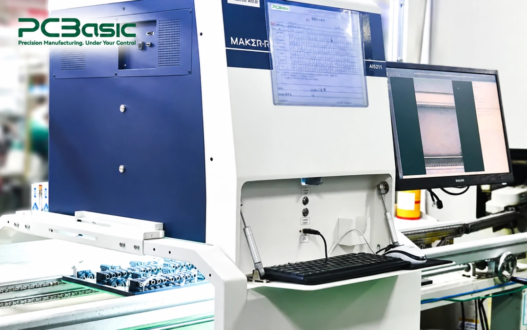
The photo is that AOI station. The boards are on the conveyor at the left, and the screen is the camera check. This one runs before the oven. After the board is soldered, AOI looks again. A bridge or a tombstone can show up on that camera. Joints under a BGA need X-ray, because this camera cannot see them.
SPI, AOI, and X-ray sit at a known point in the PCBA manufacturing process. SPI comes after the paste is printed. Pre-reflow AOI comes before soldering. Post-reflow AOI and, where required, X-ray inspection come after soldering.
Ask for the SPI result and the AOI result on the first board. These are the PCBA quality control records for that build. If the board has a BGA, ask for the X-ray image as well. A longer list of solder defects is on our SMT defect list.
A finished PCBA process includes a saved test result after the board is soldered. Power-on is only the first check. If the required test was never included in the quote, the boards ship, and the fault may only show up at your customer.
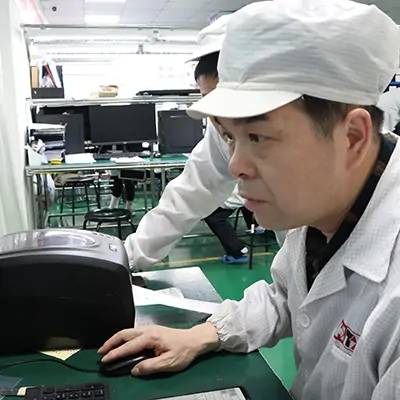
The first board is checked before volume starts. We use an in-house first-article tester for that check, and the job can include a photo of that board. Volume production starts after the first article passes.
We prepare custom test fixtures for the job. Functional testing runs before the boards are packed. It uses the limits you write down. Agree how the functional test result will be retained with the job record in our MES (the production system that tracks each step).

Write the test requirements and pass limits before you ask for the quote. Use a expected voltage and tolerance at a named test point. Use the required firmware version. Use the allowed range for idle current under stated operating conditions. With those requirements, the fixture has a clear pass and a clear fail criteria. The test types you can put in that procedure are on our PCBA functional testing page.

Four types of records help make PCBA manufacturing more predictable. You can see which part was bought. You can see the solder inspection result. You have written comments on the files before the stencil is cut. You have a test result against defined acceptance criteria. Together, these four items are the PCBA quality control record for the lot.
Send the Gerber and drill files, the BOM, the pick-and-place file, the assembly drawing, the build quantity, and the test requirements. We review that package as one manufacturing job. Start from our PCBA manufacturing services page.
Q1: What should I check first in PCBA manufacturing?
A1: Check the parts list and the solder joints. A wrong package, or a reel that is short, stops the job at incoming inspection. Bridges, tombstones, and hidden BGA joints are what SPI, AOI, and X-ray are there to catch.
Q2: Can the factory fix a board that has no test points?
A2: We can flag missing test points before the stencil is cut. We cannot add test points after the bare boards are finished. Put the test points in the design, and write the pass limits, before you ask for a quote.
Q3: Which files should I send so these problems show up early?
A3: Send the Gerber and drill files, the BOM with manufacturer part numbers, the pick-and-place file, the assembly drawing, the build quantity, and the test limits. Mark which parts may be substituted.
Assembly Enquiry
Instant Quote

Phone contact

+86-755-27218592
In addition, we've prepared a Help Center. We recommend checking it before reaching out, as your question and its answer may already be clearly explained there.
Wechat Support

In addition, we've prepared a Help Center. We recommend checking it before reaching out, as your question and its answer may already be clearly explained there.
WhatsApp Support

In addition, we've prepared a Help Center. We recommend checking it before reaching out, as your question and its answer may already be clearly explained there.
