Global high-mix volume high-speed PCBA manufacturer
9:00 -18:00, Mon. - Fri. (GMT+8)
9:00 -12:00, Sat. (GMT+8)
(Except Chinese public holidays)
Global high-mix volume high-speed PCBA manufacturer
9:00 -18:00, Mon. - Fri. (GMT+8)
9:00 -12:00, Sat. (GMT+8)
(Except Chinese public holidays)
HomePage > Blog > Knowledge Base > OSP PCB Surface Finish | A Comprehensive Guide
Copper has relatively active chemical properties and excellent electrical conductivity. However, it is prone to oxidation in the air and humid environment. The e lectrical performance and assembly reliability of PCBs are closely related to the state of the exposed copper surface. Therefore, in PCB manufacturing, to prevent the copper surface from oxidizing, a PCB surface finish is necessary.
There are various processes for PCB surface finish, such as HASL, tin plating, ENIG, ENEPIG, etc. Today, the topic of this article is OSP surface finish. We will systematically explain what OSP surface finish is, the advantages and disadvantages of OSP surface finish, etc. First, let's look at what the OSP surface finish on a PCB actually is.
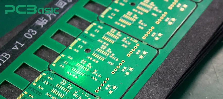
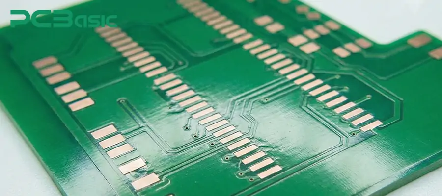
The OSP surface finish on PCB is a chemical surface finish process commonly used in PCB manufacturing to protect the exposed copper surfaces of the PCB. Its main function is to prevent the copper from oxidizing in the air and moisture environment (during manufacturing, assembly, and storage processes). Here, OSP stands for Organic Solderability Preservative, which refers to an organic protective layer specifically used to maintain the solderability of the copper surface.
In practical applications, the OSP PCB finish is a very thin organic protective film formed on the copper surface. This film acts as a barrier, isolating the copper from the air and moisture. This process does not involve metal deposition, and the original thickness and shape of the copper foil will not change. So, how does the OSP surface finish function on the PCB?
Through the previous introduction, we know that the core function of the OSP coating is to prevent the oxidation of the copper surface. Once the copper surface is oxidized, the wetting property of the solder will significantly decrease, and the soldering quality will be affected. Here is the working principle of the OSP process:
The organic molecules (usually azole compounds) in OSP are chemically adsorbed onto the copper surface, forming a uniform and firmly bonded protective layer. This layer then covers the copper surface at the molecular level, effectively blocking oxygen and moisture, thereby slowing down the oxidation rate of the copper. Moreover, the OSP protective layer is also "controllably removable" during reflow soldering.
During the reflow soldering heating process, this layer of organic film will decompose and be removed by flux activity. Once the fresh copper surface is exposed, the solder can directly wet the copper pads at the appropriate time, thereby forming a stable solder joint.
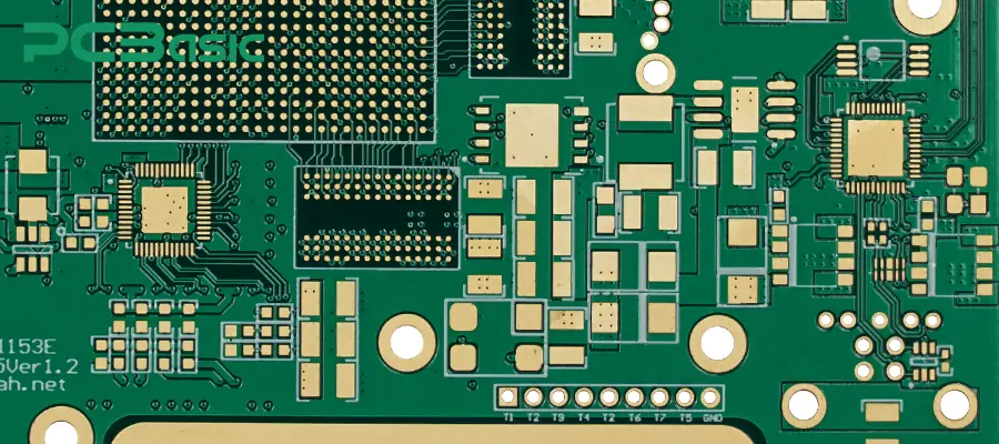
The surface finish process of OSP has multiple practical advantages in terms of soldering performance, process compatibility, and cost control.
1. High surface flatness
One of the most notable advantages of OSP PCB surface finish is that the surface is extremely smooth. This process does not involve any metal deposition, and the original shape and thickness of the copper foil can be completely retained. This feature makes OSP particularly suitable for fine-pitch devices, BGA, QFN, and high-density SMT PCB designs.
2. Initial soldering performance is good
The OSP surface finish can effectively prevent copper surfaces from oxidizing without introducing additional metallic layers or altering the original copper thickness. This ensures excellent initial solder wetting. During the reflow soldering process, the OSP protective film can cleanly decompose and be removed. The solder can directly wet the fresh copper pads. This process has good compatibility with lead-free soldering processes.
3. Cost advantage is obvious
The OSP manufacturing process is simpler compared to ENIG and ENEPIG surface finish methods. The entire process does not involve precious metals, has fewer procedures, and requires less chemical consumption.
4. Excellent environmental performance
The environmental attribute is another advantage of OSP PCB. The OSP coating does not contain heavy metals and complies with relevant environmental protection regulations such as RoHS. This enables the surface finish of OSP PCB to balance the soldering performance while also reducing environmental risks during the manufacturing process.
Overall, OSP PCB boasts excellent soldering performance, high surface flatness, as well as the advantages of low cost and environmental friendliness.
The shelf life and storage conditions of OSP PCBs are more sensitive compared to those of metal surface finishs, as the surface finish of OSP PCBs relies on an organic protective film. Understanding the shelf life of OSP PCBs and the appropriate storage methods is also a crucial aspect for ensuring reliable soldering.
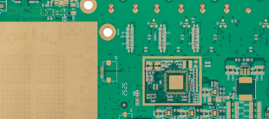
The typical shelf life of OSP PCB
Under standard manufacturing and packaging conditions, the shelf life of OSP PCBs is typically 3 to 6 months. However, the exact duration is influenced by various factors such as the type of OSP coating, process parameters, packaging method, and storage environment, so there is no fixed time. Also, please note that once OSP exceeds the recommended usage period, its protective capability will gradually decline.
Requirements for the storage environment
In order to extend the validity period of OSP PCB, the following aspects should be given particular attention in the storage environment:
Store in a dry and low-humidity environment
Avoid prolonged exposure to the air and minimize the storage time after opening
Avoid contact with sweat from hands, dust, residual fluxing agents, etc.
In actual production, vacuum or moisture-proof packaging is often used to enhance the stability of OSP PCBs during storage and transportation. Besides, pre-assembly management is also very important. Generally, it is recommended that OSP PCBs be completed with SMT mounting and reflow soldering as soon as they are opened to avoid affecting the solder wetting property due to prolonged storage.
Overall, the shelf life of OSP PCB is relatively short and it requires strict conditions for storage and handling.
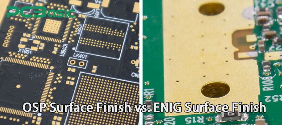
Earlier, we mentioned that there are various surface finish processes for PCBs. Among them, the one most often compared to OSP surface finish is ENIG surface finish. Both have differences in structural form, process characteristics, soldering performance, and applicable scenarios. The following table shows some comparisons between OSP and ENIG in certain aspects:
|
Comparison Item |
OSP Surface Finish |
ENIG Surface Finish |
|
Surface finish type |
Organic solderability preservative coating |
Electroless nickel/immersion gold (metallic finish) |
|
Structure |
Organic molecular layer directly on bare copper |
Multilayer structure: copper/nickel/gold |
|
Surface flatness |
Very high |
High (affected by nickel and gold layers) |
|
Soldering mechanism |
OSP film decomposes during reflow, solder wets fresh copper |
Solder wets the gold layer and reacts with nickel to form intermetallic compounds |
|
Initial solderability |
Good |
Very stable |
|
Multiple reflow capability |
Limited; typically suitable for one or two controlled reflow cycles |
Excellent; suitable for multiple reflow cycles |
|
PCB shelf life |
Shorter (typically 3–6 months) |
Longer (typically 9–12 months or more) |
|
Storage sensitivity |
Sensitive to humidity and air exposure |
High storage stability |
|
Precious metals used |
No |
Yes (nickel and gold) |
|
Cost level |
Low |
Higher |
|
Environmental characteristics |
Heavy-metal-free, RoHS-compliant |
Metallic plating process requiring strict chemical control |
|
Typical applications |
Consumer electronics, high-density SMT, high-volume production |
Automotive electronics, industrial control, high-reliability products |
In summary, OSP finish on PCB emphasizes low cost, high flatness and good initial soldering performance. In contrast, ENIG surface finish places more emphasis on soldering consistency, storage life and reliability.
There is no absolute superiority or inferiority between OSP surface finish and ENIG surface finish. If the product aims for cost control, large batch production, and a short time to market, choosing OSP PCB is more advantageous. However, if the product has high requirements for soldering reliability, storage period, or multiple reflow soldering, ENIG is a more reliable choice.
The application of OSP surface finish is very extensive, but it is not suitable for all scenarios. In the following scenarios, it is very appropriate for us to use the OSP surface finish process on PCBs.
1. Cost-sensitive PCB projects
When a project has high requirements for cost control, OSP PCB finish is usually a more suitable choice. This is because the OSP process is relatively simple and does not involve precious metals such as nickel and gold, resulting in low material costs. This is particularly suitable for large-scale consumer electronics products.
2. High-density, fine-pitch SMT design
OSP surface finish is highly suitable for fine-pitch devices, high-density SMT layouts, and small-sized passive components. This is because the OSP coating forms an extremely thin and smooth organic protective film on the copper surface, which is very flat. And surface flatness is an important advantage of PCB OSP in modern mounting processes.
3. Single or limited reflow soldering process
OSP is suitable for scenarios where only one reflow soldering or a controlled number of thermal cycles are required. Because the OSP coating will decompose and be removed during the reflow soldering process, multiple high-temperature reflows will reduce the soldering reliability of the PCB.
4. PCB manufacturing projects with shorter delivery deadlines
The OSP manufacturing process has a shorter cycle and fewer chemical finish and electroplating steps, making it suitable for prototyping and quick production.
5. Products with controllable storage and assembly conditions
The storage time of OSP PCBs is relatively limited, and they are more suitable for the following scenarios:
After PCB is manufactured, it can quickly enter the assembly process.
The temperature and humidity in the storage environment can be controlled.
There is no need for long-term inventory storage.
6. Environment-friendly manufacturing requirements
OSP uses fewer heavy metals and has lower levels of chemical waste and heavy metal emissions, making it more environmentally friendly.
When the project possesses the above characteristics, OSP surface finish on the PCB will be a very suitable choice.
1. How long can an OSP PCB be stored without affecting the soldering process?
In a sealed, dry, and low-humidity environment, an OSP PCB can typically be stored for 3 to 6 months. If the packaging is opened or exposed to a high-humidity environment, the effective storage time will significantly shorten.
2. How to determine if the OSP PCB soldering has been affected?
If the copper surface of the OSP PCB becomes darker, the solder paste wetting becomes poor, or it requires an increased reflow temperature to achieve proper soldering, this usually indicates that the soldering has been affected.
3. Can OSP PCB be used after getting damp?
It depends on the specific situation. For a slightly damp OSP surface finish, the soldering performance can be partially restored by low-temperature baking the board. However, if the copper surface has obvious oxidation or has become dark, this indicates that the OSP has failed and it is not recommended to use it.
4. Is OSP suitable for manual soldering or rework?
Not recommended. Because the OSP finish on the PCB is removed after one reflow soldering process. The bare copper is prone to oxidation. Then, during manual soldering or multiple rework processes, the consistency and wetting of the solder joints will be compromised.
OSP PCB is a surface finish method in PCB manufacturing. It achieves a good balance between cost, solderability and process efficiency, and is widely used. However, it also has some limitations, such as being unsuitable for long-term storage. Therefore, when choosing the OSP process, it should be determined based on specific circumstances. Overall, when the project focuses on cost, flatness, production efficiency, and environmental protection requirements, and can ensure good storage and assembly conditions, OSP finish on PCB is a very suitable choice.
Time is money in your projects – and PCBasic gets it. PCBasic is a PCB assembly company that delivers fast, flawless results every time. Our comprehensive PCB assembly services include expert engineering support at every step, ensuring top quality in every board. As a leading PCB assembly manufacturer, we provide a one-stop solution that streamlines your supply chain. Partner with our advanced PCB prototype factory for quick turnarounds and superior results you can trust.
Assembly Enquiry
Instant Quote
Phone contact

+86-755-27218592
In addition, we've prepared a Help Center. We recommend checking it before reaching out, as your question and its answer may already be clearly explained there.
Wechat Support

In addition, we've prepared a Help Center. We recommend checking it before reaching out, as your question and its answer may already be clearly explained there.
WhatsApp Support

In addition, we've prepared a Help Center. We recommend checking it before reaching out, as your question and its answer may already be clearly explained there.