Global high-mix volume high-speed PCBA manufacturer
9:00 -18:00, Mon. - Fri. (GMT+8)
9:00 -12:00, Sat. (GMT+8)
(Except Chinese public holidays)
Global high-mix volume high-speed PCBA manufacturer
9:00 -18:00, Mon. - Fri. (GMT+8)
9:00 -12:00, Sat. (GMT+8)
(Except Chinese public holidays)
HomePage > Blog > Knowledge Base > Integrated Circuits (ICs): Structure, Types, and Applications
In the digital age today, integrated circuits are everywhere. They appear in smartphones, car control systems, household appliances, medical devices and even satellites. Without IC chips, modern IC electronics cannot operate properly. These small but powerful microchips make computing, communication, control and intelligent technologies possible.
From the earliest transistors to today's high-density IC chips integrating billions of devices, the continuous progress of integrated circuits has driven the development of the information age. In this guide, we will introduce what an integrated circuit is, understand the structure and function of IC components, and take a look at different types of IC packages. Understand the manufacturing process of electronic integrated circuits and explain why IC chips are indispensable in modern life.
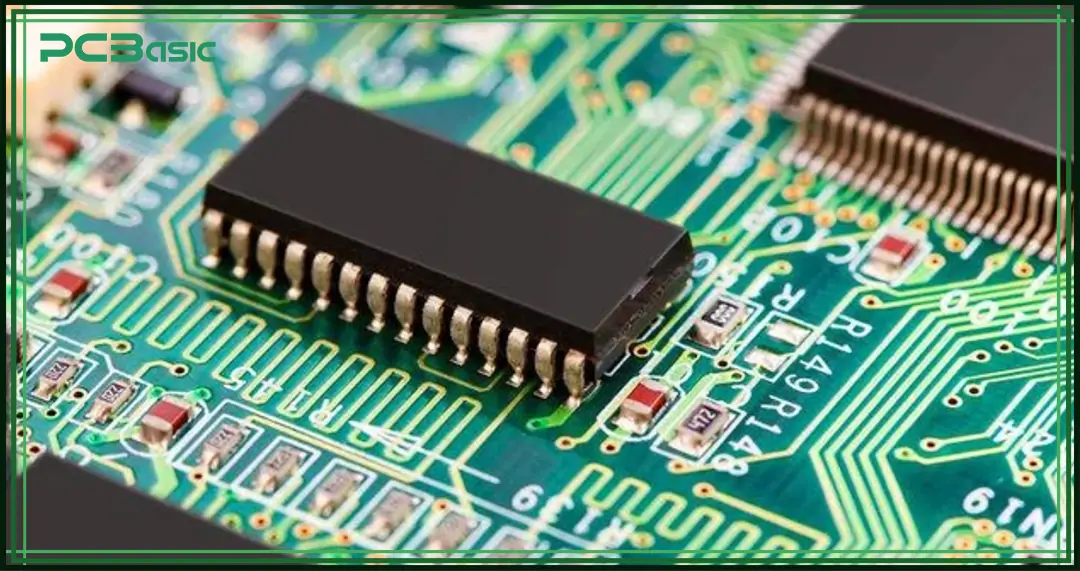
An integrated circuit (IC), also known as a microchip, IC chip or electronic integrated circuit, is a small piece of semiconductor material, usually made of silicon.
The name integrated circuit indicates that it integrates multiple electronic components on a single chip. This can significantly reduce the volume of the circuit and lower power consumption and costs while enhancing performance and reliability.
Inside this chip, there are thousands or even billions of tiny IC components, which include transistors, resistors, capacitors and diodes. These components are connected together through circuits to perform various electronic functions. Inside a typical IC chip, transistors are used to control the switch, resistors regulate the current, capacitors store and filter charges, and diodes are responsible for controlling the direction of the current.
IC electronics powers almost all modern electronic products, such as computers, smartphones, automobiles, medical devices and industrial control systems. Without ICs, these technological devices simply cannot function properly.
Integrated circuits can be classified into different types according to their functions and designs.

Analog integrated circuits are used to handle continuous signals. The output will change along with the variation of the input signal. Common applications include audio amplifiers, RF amplifiers, temperature sensors and power management.
In analog IC electronics, IC components are used to process various real-world signals such as sound, light and temperature.
Digital integrated circuits operate with binary signals. The signals only have two states: ON (logic 1) or OFF (logic 0). These IC chips are the core of modern computing and communication systems. They are commonly found in microprocessors, microcontrollers, logic gates and memory chips (such as RAM and ROM).
Digital IC electronics enable computers, servers, smartphones and network devices to complete various complex processing tasks.
Mixed-signal integrated circuits combine analog circuits and digital circuits simultaneously on an IC chip. Common applications include analog-to-digital converters, digital-to-analog converters, clock generators and sensor interfaces.
These microchips are suitable for use in audio devices, data converters and wireless communication systems, as these applications need to process two different types of signals simultaneously.
The history of integrated circuits can be traced back to 1947. At that time, John Bardeen, William Shockley and Walter Bratton invented the transistor. This invention made electronic devices smaller and more efficient, which laid the foundation for the later integrated circuits.
In 1958, Jack Kilby of Texas Instruments and Robert Noyce of Fairchild Semiconductor independently developed the first integrated circuit. They integrate multiple IC components on a single silicon chip, eliminating the need for complex wiring to connect individual components.
Since then, electronic integrated circuits have made rapid progress with higher and higher levels of integration:
• Small-Scale Integration (SSI): Each IC contained dozens of transistors.
• Medium-Scale Integration (MSI): Hundreds of transistors on one chip.
• Large-Scale Integration (LSI): Thousands of transistors.
• Very-Large-Scale Integration (VLSI): Millions of transistors.
It is precisely because of these technological advancements that today's integrated circuits can drive the operation of supercomputers, smartphones, self-driving cars and artificial intelligence systems. The shrinking size of ic components follows Moore's Law, where the number of transistors doubles about every two years.
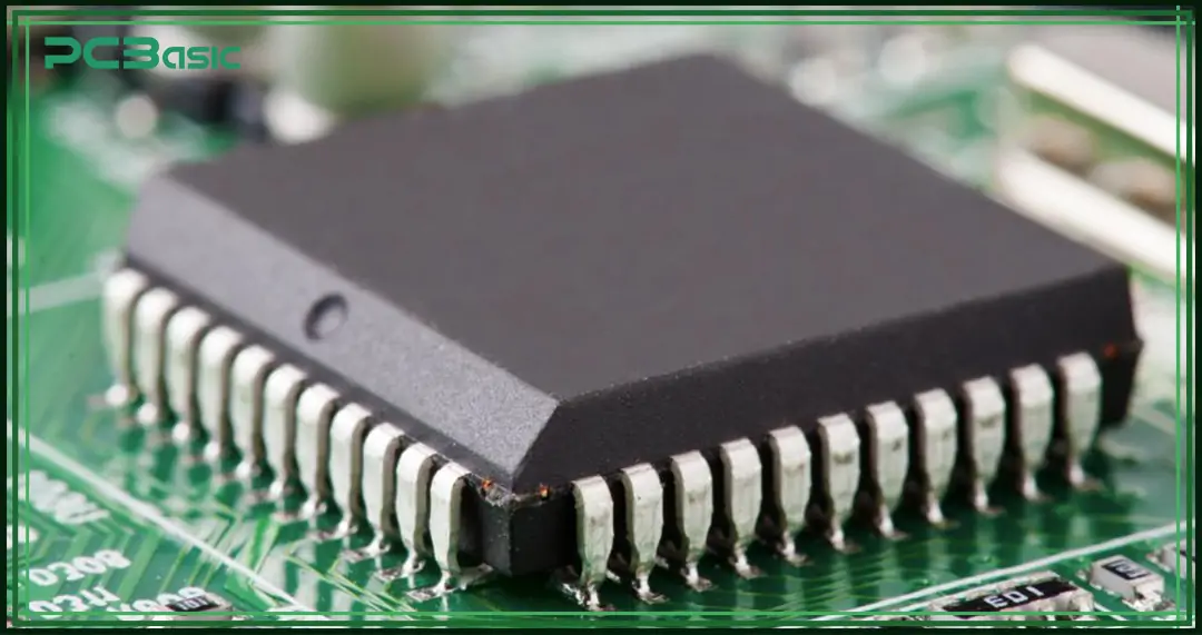
When an integrated circuit die is made, it needs protection and must connect to the outside. This is where IC packages are used. An IC package holds the IC, protects it from damage, and gives electrical contacts to connect with other IC components and the circuit board.
Dual In-line Package (DIP)
This is a classic through-hole package. It has two rows of pins. It is often used for prototypes and early microcontrollers.
Small Outline IC (SOIC), SSOP, TSSOP
These are surface-mount packages. They are good for small and compact designs.
Quad Flat Package (QFP), Thin QFP (TQFP)
The pins come out from all four sides. These are often used in microcontrollers and processors.
Quad Flat No-Lead (QFN), Dual Flat No-Lead (DFN)
This type of IC package has exposed pads on the bottom, which help with heat dissipation.
Ball Grid Array (BGA)
This package has balls of solder on the bottom. It offers very high connection density. It is used in advanced CPUs, GPUs, and FPGAs.
The choice of IC package depends on the chip's function, size, heat needs, and how it fits into the IC electronics system.
 About PCBasic
Time is money in your projects – and PCBasic gets it. PCBasic is a PCB assembly company that delivers fast, flawless results every time. Our comprehensive PCB assembly services include expert engineering support at every step, ensuring top quality in every board. As a leading PCB assembly manufacturer, we provide a one-stop solution that streamlines your supply chain. Partner with our advanced PCB prototype factory for quick turnarounds and superior results you can trust.
Each integrated circuit has identification markings. These include:
• Manufacturer logo
• Part number
• Date code
• Integrated circuit symbol to show pin 1 (marked with a dot or notch)
These markings help technicians install and check IC components correctly in complex systems.
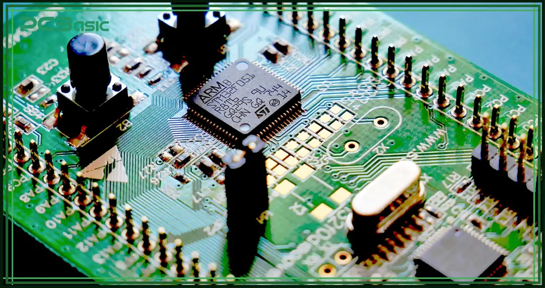
Inside the black plastic IC package, the real IC chip (usually called the die) has many tiny layers. The structure is very complex:
• Semiconductor Layer: The bottom layer. It uses high-purity silicon as the base of the chip.
• Doping Layer: Adds impurities to form N-type and P-type areas to make transistors.
• Metal Interconnect Layer: Copper or aluminum lines connect different IC components.
• Insulation Layer: Silicon dioxide separates the active layers.
• Passivation Layer: The top protective layer that prevents damage.
The design process of integrated circuits usually includes these steps:
• Architecture Design: Define the chip's function, speed, power, and size.
• Logic and Circuit Design: Build logic blocks using transistors and logic gates.
• Physical Design: Arrange the position and wiring layout of IC components.
• Verification: Check if the design is correct, manufacturable, and meets performance.
• Signoff: Final check before manufacturing to make sure everything is ready.
Modern IC electronics design uses Electronic Design Automation (EDA) software. These tools help create complex IC chips with billions of IC components.
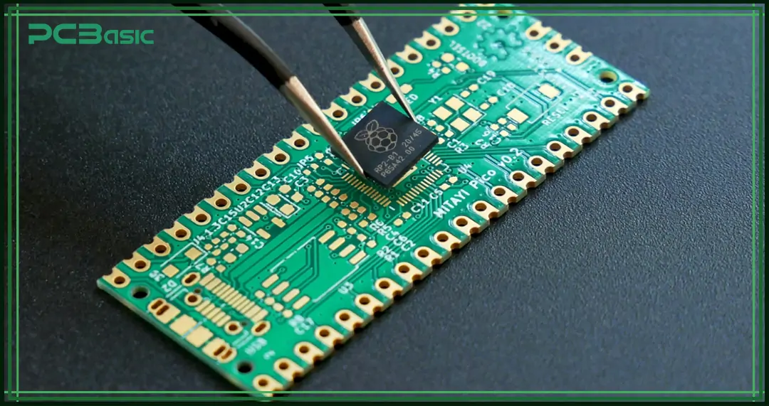
The manufacturing process of integrated circuits is one of the most advanced and complex manufacturing technologies in the world. Below is the main process of making IC chips:
1. Wafer Production
First, high-purity silicon ingots are grown using the Czochralski process. These silicon ingots are extremely pure and serve as raw materials for making integrated circuits.
Then, the silicon ingots are sliced into very thin round silicon wafers. The surface of each wafer is polished to become very smooth, preparing it for further processing.
2. Photolithography
A layer of photoresist is applied to the wafer. Then, light is used to transfer circuit patterns onto the photoresist layer.
After exposure, the photoresist is developed, leaving behind patterns needed for the circuit. These patterns mark the positions of future IC components.
3. Doping and Ion Implantation
Doping elements are injected into specific areas on the wafer surface. These dopants change the electrical properties of silicon, creating N-type and P-type regions.
In this way, transistors that control the flow of current are made. These transistors are one of the basic IC components in integrated circuits.
4. Thin Film Deposition and Etching
Very thin metal layers (like copper or aluminum) are deposited on the wafer to serve as conductors in the circuit. Dielectric layers are also deposited to separate different wires.
Then, etching is used to shape the metal layers into interconnecting lines, connecting different IC components and forming a complete circuit.
5. Layer Stacking
This process is repeated many times. Each layer contains different wires and IC components.
By stacking layers one by one, complete and complex electronic integrated circuits are formed to support various functions.
6. Packaging
After wafer fabrication, the wafer is cut into individual dies. Each die is a complete IC chip.
The dies are tested. Qualified ones are packaged into proper IC packages. The package protects the chip and makes it easier to mount on circuit boards.
7. Testing
Before shipping, every IC chip must go through strict functional, thermal, and electrical testing. These tests make sure each IC chip works properly and meets factory standards.
With this precise manufacturing process, factories can create billions of transistors at the nanometer scale, producing advanced microchips that power today's IC electronics devices.
Integrated circuits are one of the most important and revolutionary inventions in human history. Inside these tiny IC chips are many complex IC components. These chips power almost all the technology we use today. From smartphones and computers to life-saving medical devices, self-driving cars, and advanced artificial intelligence systems — all rely on them.
As integrated circuits keep improving, their size becomes smaller, but their performance keeps getting stronger. Today’s electronic integrated circuits offer much higher computing power and more functions, even as their size keeps shrinking.
The technology for IC electronics design, structure, manufacturing, and IC packages is now extremely advanced. Because of these high-level technologies, modern life is faster, smarter, and more connected than ever before.
Assembly Enquiry
Instant Quote
Phone contact

+86-755-27218592
In addition, we've prepared a Help Center. We recommend checking it before reaching out, as your question and its answer may already be clearly explained there.
Wechat Support

In addition, we've prepared a Help Center. We recommend checking it before reaching out, as your question and its answer may already be clearly explained there.
WhatsApp Support

In addition, we've prepared a Help Center. We recommend checking it before reaching out, as your question and its answer may already be clearly explained there.