Global high-mix volume high-speed PCBA manufacturer
9:00 -18:00, Mon. - Fri. (GMT+8)
9:00 -12:00, Sat. (GMT+8)
(Except Chinese public holidays)
Global high-mix volume high-speed PCBA manufacturer
9:00 -18:00, Mon. - Fri. (GMT+8)
9:00 -12:00, Sat. (GMT+8)
(Except Chinese public holidays)
HomePage > Blog > Knowledge Base > IC Package Types: Your Ultimate Guide
IC packages contain silicon chips or are designed to encapsulate them. The Integrated Circuit package’s main purpose is to protect the smaller components located on a circuit board. Therefore, they are very common in the printed circuit board industry. IC packaging is incorporated in different circuit boards following product requirements.
What are you going to learn in this article? This is a comprehensive article which will share authentic knowledge about the following topics:
1. What is an IC package?
2. Types of IC packages
3. Chip-Scale Package (CSP)
4. Pin Grid Array (PGA)
5. Land Grid Array (LGA)
It is very important to know that each package type is not for a single purpose. They have different designs and serve a particular purpose. So the right package is crucial in making the right design. Moreover, applications are also different. Let’s read about each in detail.
Have you seen a computer chip in your personal computer during cleaning or blowing? Although it is very small in size, the whole computing process runs through it. However, it is very delicate. The same is the case with the IC packages. These packages perform two functions:
1. Protection
2. Connection
The shell of the IC package is very strong because its core purpose is to protect the internal parts from shocks and moisture.
Similarly, these packages maintain a seamless connection. They have pins that connect the different chips to streamline the current flow.
So how can you conclude this? An IC package is a protective coating that also establishes a connection among different parts.
There are different types of IC packages, such as SOIC packages and dip packages. You have read previously that every package is built for a particular function. Below, you are going to read the most common types of packages in easy language.
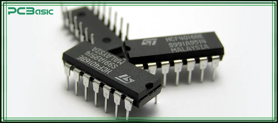
DIP is a classic example of an IC package. Earlier, circuit board manufacturers used dual in-line packages to make circuit boards. It is in a rectangular shape with two rows of pins. These pins are easy to connect with a PCB. Since it has a basic interface, it is good for beginners to make prototypes.
There are some passive sides also. For example, DIPs are bigger in size. Modern devices require smart components. However, they are still in many devices where space is not a big problem.
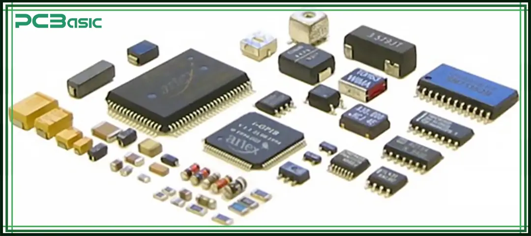
SMD packages are more advanced. If you compare them with DIP, the surface mount device is not only light, but you can also install it effortlessly.
In the SMD package, one popular type is SOIC. If we talk about its shape, it is rectangular. Moreover, it has pins on two sides. In modern LEDs, SOIC is in high demand because you can easily install them on circuit boards. In addition, they can be customized too. For example, you can add pins to fit the package to make it fit any size.
QFP packages have more space to install further connections. For example, in the quad flat package, there are leads on four sides. So you can conveniently install chips with a lot of pins. One of the major beneficiaries of such packages is microcontrollers. They also come in different sizes. You need to choose which best suits the project.
Now there is a little change in the structure of IC packages. For instance, in previous packages, the parts had pins on their sides. In the Ball Grid Array, you will see small balls. Interestingly, BGAs have more space for pin connections. They are pretty tightly packed. The most common applications are computer GPUs and CPUs.
In advanced computers with higher GPU capacity like Nvidia, PCB companies are installing attest BGA packages.
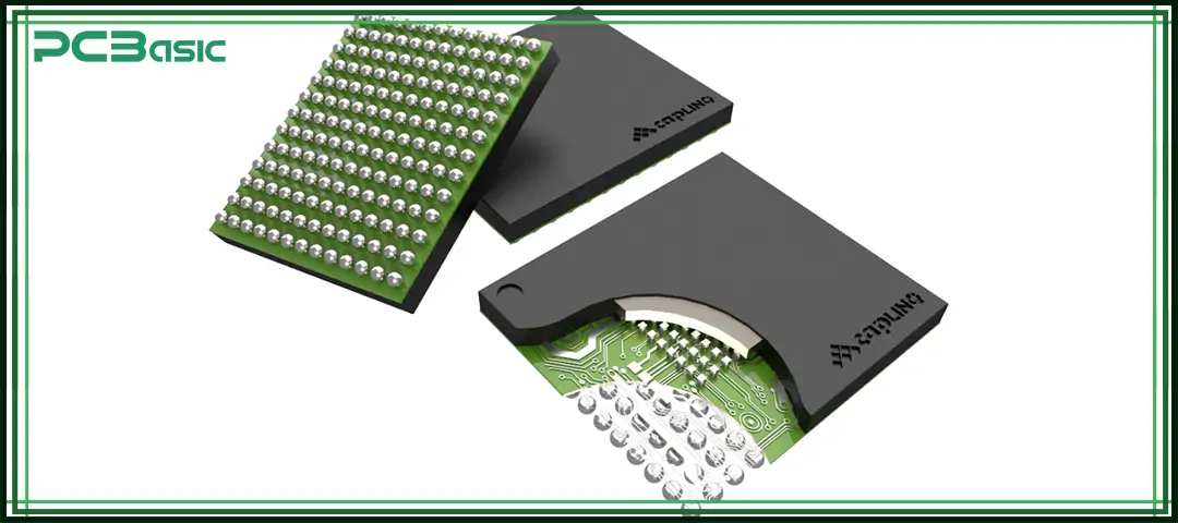
CSP packages are very small. You can say their size is similar to the chip. However, chip scale package performance outweighs other package options. Simultaneously, you can easily integrate them with any circuit board. The major applications are medical implants, wearables, and smartphones.
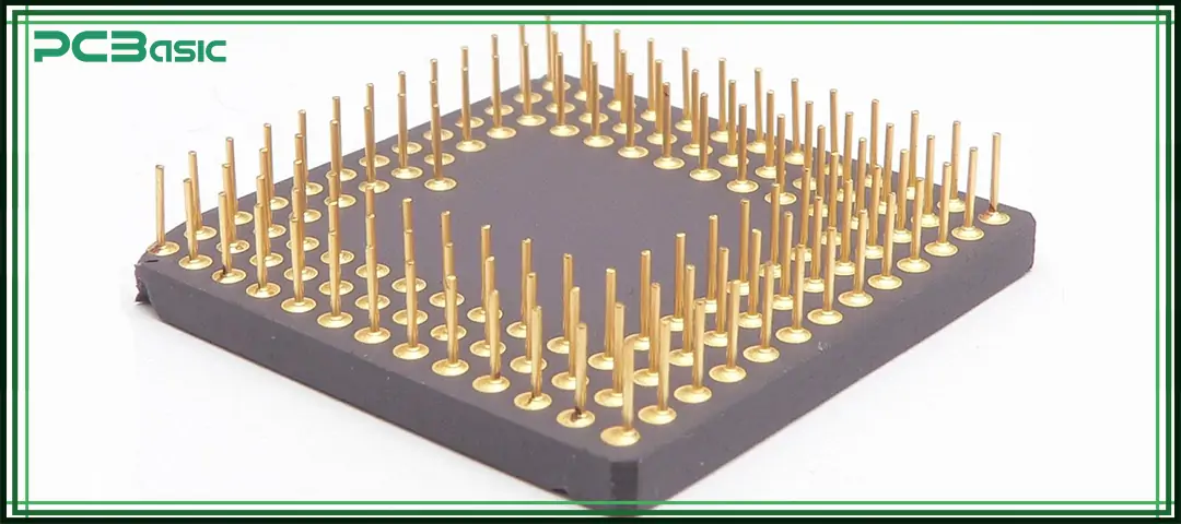
The PGA package has pins on the bottom. Since it is different in size and also provides customization, you can integrate more robust chips such as microprocessors. Subsequently, you can install them in sockets. Furthermore, the Pin Grid array can also be modified. However, there are some disadvantages too. For example, some PGAs generate significant heat, they need separate heat sinks to keep them cool
 About PCBasic
Time is money in your projects – and PCBasic gets it. PCBasic is a PCB assembly company that delivers fast, flawless results every time. Our comprehensive PCB assembly services include expert engineering support at every step, ensuring top quality in every board. As a leading PCB assembly manufacturer, we provide a one-stop solution that streamlines your supply chain. Partner with our advanced PCB prototype factory for quick turnarounds and superior results you can trust.

If we talk about the structure of LGA, they have contact pads. These pads are good for a seamless connection. You won’t find any pins there. Land grid arrays are good for powerful chips. Moreover, thermal efficiency is beyond your thoughts. PCB manufacturers ensure special safety protocols to avoid any damage.
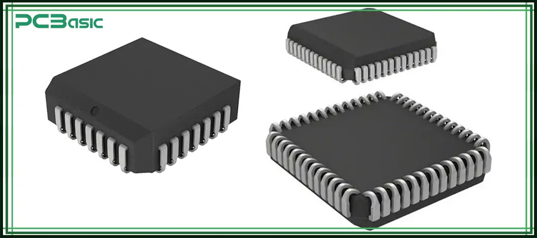
PLCC's shape is distinctive. It has a j shape leads around the corner edges. They help in surface mount components. These days, PLCCs are less common in modern applications, however, in older technology, they are still in use.
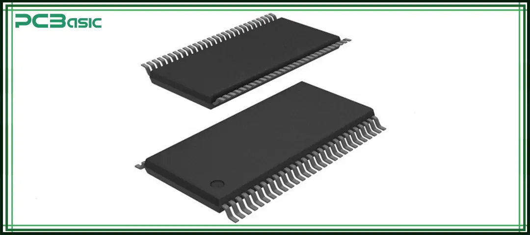
You can think TSOP is similar to the SOICs package. However, the first is thinner in size. The thin, small outline package fits perfectly in tight areas. Generally, such packages are incorporated in flash memory and computer RAMs.
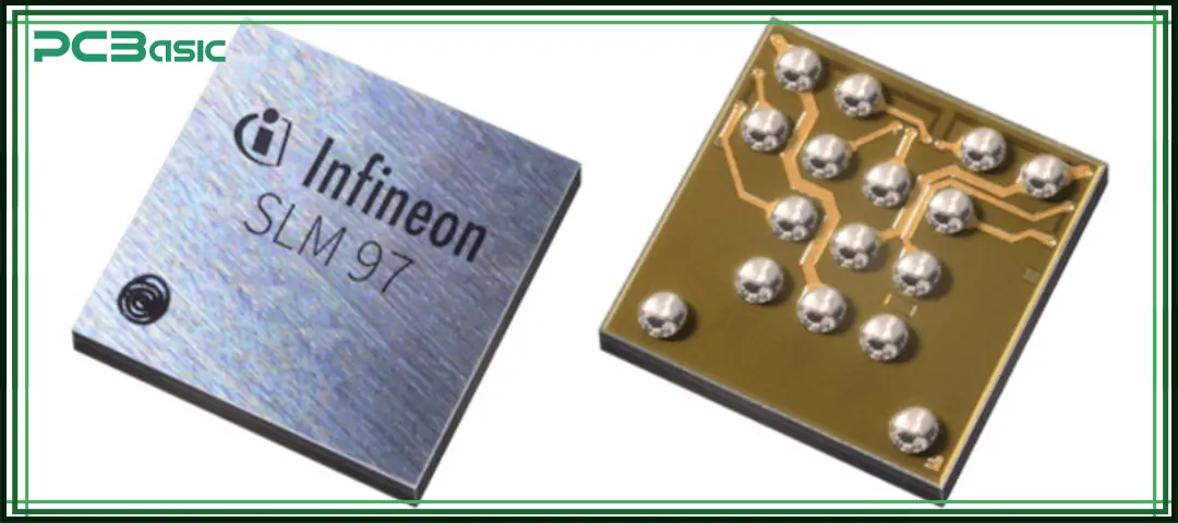
WLCSP packages are dominating the circuit board industry because it is the most advanced form. You can also see that the name shows that the packaging moves at the wafer level. What does it mean? It shows that these packages are very small and can fit in any size. However, PCB companies need special tools and skills to install this package.
|
IC Package Type |
Advantages |
Shortcomings |
Junction-to-Case Thermal Resistance (θJC) |
Junction-to-Air Thermal Resistance (θJA) |
Operating Temperature Range(°C) |
|
DIP |
Easy to install |
Insufficient thermal performance |
~10-30°C/W |
~50-100°C/W |
-40°C to 85°C |
|
QFP |
- High I/O density. |
- Fragile leads |
~2-5°C/W (with heat sink)~20-40°C/W |
~30-80°C/W |
-40°C to 85°C |
|
BGA |
- Very high I/O density. |
- Expensive. |
~1-5°C/W |
~15-50°C/W |
-40°C to 85°C (Commercial)-55°C to 125°C |
|
PLCC |
- Compact size. |
Moderate thermal performance |
~20-30°C/W |
~40-80°C/W |
-40°C to 85°C |
|
TQFP |
- Very thin and compact. |
- Leads are fragile |
~10-25°C/W ~30-50°C/W |
~40-70°C/W |
-40°C to 85°C |
|
CSP |
- Extremely small size |
- Expensive. |
~1-5°C/W |
~10-30°C/W |
-40°C to 85°C |
|
Flip-Chip Package |
short interconnects |
- Complex manufacturing process |
~0.1-2°C/W |
~5-20°C/W |
-40°C to 85°C |
|
SOIC |
- Smaller footprint than DIP. |
- Moderate I/O count. |
~10-30°C/W |
~40-100°C/W |
-40°C to 85°C |
|
LCC |
- No fragile lead |
- Heat dissipation is limited |
~10-20°C/W |
~40-80°C/W |
-40°C to 85°C |
|
LGA |
- High I/O density. |
- Complex assembly |
~1-5°C/W |
~20-50°C/W |
-40°C to 85°C |
Till now, you have read everything about types of IC packages. Understanding the basic concepts of IC packaging will help you to choose the right package type. PCBasic is a leading circuit board manufacturer. Our companies have seasoned experts who can incorporate these packaging following circuit board requirements.

Assembly Enquiry
Instant Quote
Phone contact

+86-755-27218592
In addition, we've prepared a Help Center. We recommend checking it before reaching out, as your question and its answer may already be clearly explained there.
Wechat Support

In addition, we've prepared a Help Center. We recommend checking it before reaching out, as your question and its answer may already be clearly explained there.
WhatsApp Support

In addition, we've prepared a Help Center. We recommend checking it before reaching out, as your question and its answer may already be clearly explained there.