Introduction
A dual inline package is a common component package in electronics comprising a PCB. Understanding the dual inline packaging meaning and associated details is very important to have an idea of its functioning and significance. You are at the right place if you look forward to knowing about the DIP package. The guide below covers the DIP chip's purpose, meaning, history, and more. So, let's read below.
Dual Inline Package Meaning (What is Dual inline Package)
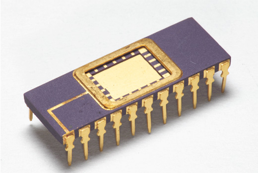
The dual inline package is an IC package in electronics consisting of PCB. Dual inline package is commonly abbreviated as DIL or DIP. DIP chip manufacturing comprises epoxy resin by melting and molding it and then leaving it to rest in a frame with connecting pins incorporated. These pins extend out vertically from the frame. The parallel pins consist of gold, tin, or silver plating.
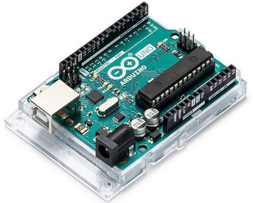
These dual inline packages are mounted on the PCB or inserted by the through-hole technique; they can also be fixed within a socket.
The DIP chip may contain a different number of pins. A DIP chip is represented by the number of pins present within it. For instance, a dual inline package containing eight pins each on two of its rows will have a total of 16 pins, and it would be referred to as DIP16; the one with eight pins on the whole will be called DIP8, and so on.
The number of pins also determines the size of the DIP package. The common number of DIP package pins is 4, 6, 8, 10, 12, 14, 16, etc. Moreover, these pins have different pitches depending on the types of boards they are inserted into, and these may vary between 0.5mm, 0.65mm, 2.54mm, etc.
Structure of Dual Inline Package
The essential elements in the structure of a DIP include a lead frame, silicon die, polymer mold, package substrate, and wire bonds of gold.
The lead frame of the DIP is the main component that ensures the electrical connections are intact and hold the silicon die. An insulation material, a thick package substrate, helps to support the lead frame electrically.
The major component of the DIP package is the silicon die because it has the electronic circuitry that carries out the required functions and processes. On the other hand, wire bonds of gold connect the silicon die and the lead frame to let the electoral signals flow between the external world and the silicon die.
The lead frame also has an added coating of polymer overmold, which protects the components within it. It helps to improve the reliability of the dual inline package. It also keeps the moisture away from getting into the frame.
 About PCBasic
Time is money in your projects – and PCBasic gets it. PCBasic is a PCB assembly company that delivers fast, flawless results every time. Our comprehensive PCB assembly services include expert engineering support at every step, ensuring top quality in every board. As a leading PCB assembly manufacturer, we provide a one-stop solution that streamlines your supply chain. Partner with our advanced PCB prototype factory for quick turnarounds and superior results you can trust.
Features of a Dual Inline Package
The dual in-line package comprises soldering them with the circuit boards, so attention should be paid to the placement and positioning of the pins. Some of the essential features of a DIP package are as follows:
Spacing
According to the JEDEC standards, which are used for internationally accepted DIP packages, the two pins must have a pitch of 2.54 mm. The DIP package, used in certain eastern countries, comprises a standard different from JEDEC, and the pitch is 2.5mm. The number of pins determines the distance between the rows of pins.
Number of Needles
The number of pins found in a dual inline package follows a pattern of even numbers, and hence, the count of these pins is a multiple of 2, like 8, 14, 16, 20, and so on. DIP packages could comprise 52 to 64 pins, which are the maximum pin counts used widely by the DIP packages manufactured these days.
Orientation and Number of Pins
The position of the identification notch of the DIP components determines the position of the pins. If it faces up, the first pin on the upper left is pin number 1, and the rest are organized anti-clockwise.
Let's take an example of a DIP18 IC: the identification notch is upward-facing, and the pins on the left are 1 to 9 from top to bottom. At the same time, the right side has bottom-to-top pins, which are ranging from 10 to 18.
Pros of DIP
● The DIP package is affordable and simple in structure with no complex layouts leading to additional cost.
● They are highly suitable for a huge production volume because of their easy manufacturing process.
● They suit well with the through-hole mounting methods.
● DIP packages also offer efficient heat dissipation and help avoid overheating issues.
● They are easily replaceable and, during replacement, do not damage the components in their surroundings.
Cons of DIP
● Compared to other packaging types, DIP needs more space on the circuit board.
● Applications equipped with high density may not find DIP suitable because of the limited pin spacing.
● The strength of DIPs is lacking when compared to other types of packaging, and if subjected to bending and twisting, they can get damaged.
● Temperature changes may impact the DIPS, leading to solder joint failure because pins may expand or contract.

How to Install DIP Packages?
The first stage is drilling holes in the positions reserved for the DIP package, and these holes should correspond to the number of pins and through holes. The pins are then fixed into the holes and are soldered with the board.
The entire process of fixing the DIP packages is straightforward. However, the process must be done carefully when removing and inserting chips so the pins are not damaged.
Apart from mounting through hole-punch, you can consider mounting through DIP sockets. The IC of DIP is removed or fixed into the circuit board with the help of a socket.
History of Dual Inline Package

The dual inline package was invented by three people, namely, Rex Rice, Don Forbes, and Bryant Rogers, in 1964. They considered this invention because of the limitation observed in using ICs due to limited leads on the circuit.
The circuits were becoming increasingly complex, so they needed sufficient signals to work with the complex electronic devices. By developing the DIP package, high-density chip carriers came into being and are even easily fixed on the PCBs.
Variants of DIP Package (Types)
Single in-line Package
A single in-line package is a package in which a pin row has been removed, comprising a smaller footprint. The row of removed pins can be replaced with a heat sink to improve the power parameters.
Dual in-line Package
The dual in-line package comes with multiple variants, as discussed below:
Plastic dual in-line package, also known as PDIP, is one of the cheapest options because plastic materials are cheaper. Hence, it supports savings when manufacturing DIPs in high volume. It has two rows of pins in parallel, offering protection and insulation for the integrated circuits.
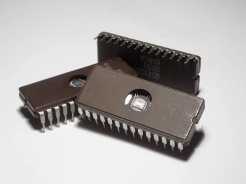
On the other hand, the
ceramic dual in-line package supports EPROM and consists of a quartz window that can erase the chip using ultraviolet light. CDIP offers efficient performance and resistance against moisture, shock, and heat conditions.
Shrink or skinny dual in-line package comprises space-saving options. The skinny ones may have half the row spacing, whereas the shrink ones may reduce the pin pitch by 30 percent. Skinny DIP comprises a pin center distance of 2.54 mm and a width of 7.62 mm, and shrink DIP comprises a 0.07-inch small lead pitch (1.778mm).
Quad in-line packaging, conversely, comprises additional rows on each side of the DIP made of pins. These rows improve PCBs' working functionality and solderability with single sides.
Dual Inline Package Applications
DIP packaging is most commonly used in integrated circuits. You'll see the DIP design in most electronic and computing devices like DIP switches, strip displays, LEDs, seven-segment displays, and relays.
The very first DIP package components were invented in 1964; it had a component that consisted of 14 pins and looked much similar to the DIP packaging components that are used today. The older versions consisted of round components, which are now replaced by rectangular ones so that the density of the component may increase.
DIP packaging components are also used in the automated assembly equipment, and the board can have hundreds of ICs. If the size of the DIP components matches the size of the ICs inside them, they will have a larger size.
Due to the evolution of SMT packaged components at the end of the 20th century, the size and weight of the entire system were meant to be reduced.

DIP vs. SOP Packages
SOP, standing for small outline package, is another package that comprises two terminal directions. The terminals of the SOP package are L-shaped.
Keeping the number of pins the same, the SOP package is usually smaller in size, while the DIP package takes more space. Hence, the SOP helps reduce space consumption by thirty to forty-five percent and can reduce a massive amount of thickness.
Hence, SOP is a compact version of the DIP package and is a commonly used SMT technology in most consumer electronics.

Conclusion
As you have read the guide above, you must know the dual inline package meaning, its pros and cons, applications, history, and types. Choosing the right DIP package supplier like PCBasic may help you develop and manufacture better electronic products that last longer and perform efficiently.
Looking for a PCB or PCBA quote? Contact us now.

 About PCBasic
