Global high-mix volume high-speed PCBA manufacturer
9:00 -18:00, Mon. - Fri. (GMT+8)
9:00 -12:00, Sat. (GMT+8)
(Except Chinese public holidays)
Global high-mix volume high-speed PCBA manufacturer
9:00 -18:00, Mon. - Fri. (GMT+8)
9:00 -12:00, Sat. (GMT+8)
(Except Chinese public holidays)
HomePage > Blog > Knowledge Base > 0201 Component Size Explained: Dimensions and PCB Assembly Considerations
Electronic products are constantly evolving towards miniaturization and high integration, and the size of components is getting smaller and smaller. Small components like 0201 packages allow us to place more devices on a limited PCB area, making the layout more compact and flexible. However, this also means that the requirements for manufacturing and assembly are increasing.
Before choosing the 0201 components, we should first have a clear understanding of the 0201 component size itself. How small is the actual size of 0201? What are the differences compared with common SMD packages such as 0402? What challenges will be encountered in the PCB assembly process? Next, this article will focus on the 0201 component size.
The 0201 component is one of the smallest standardized SMD surface mount components widely used in electronic manufacturing today. The name "0201" discussed in this article refers to the imperial (inch-based) package designation, not the metric naming system.
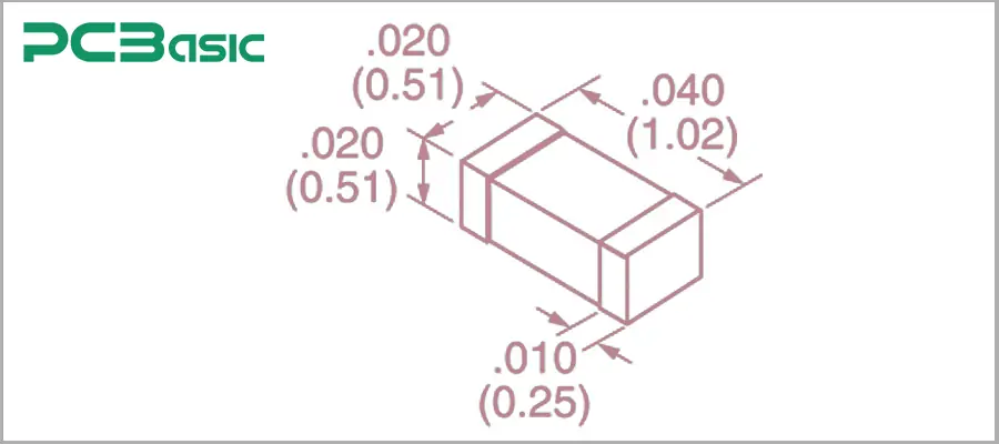
Specifically, the 0201 package indicates that the component's size is 0.02 × 0.01 inches, which converts to approximately 0.6 × 0.3 mm in the metric system. It is very important to correctly understand this point. In scenarios with high-density layouts, any deviation in size understanding can easily lead to packaging or process issues.
Dimension Conversion
0.6 mm ≈ 0.024 inches
0.3 mm ≈ 0.012 inches
This precisely corresponds to the naming logic represented by "0201". This size is extremely small, but the placement accuracy and solder paste volume must still be precise. Otherwise, it will have a significant impact on the quality and reliability of the soldering.
In practical applications, almost all 0201 components are surface mount resistors and surface mount capacitors.
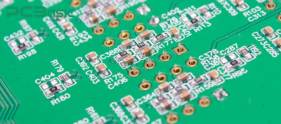
From the perspective of PCB packaging and pad design, the size of 0201 resistors is exactly the same as that of 0201 capacitors. Both adopt the same 0201 package size, and the shape, spacing and placement coordinates of the pads on the PCB are also the same.
Therefore, in high-density designs, we can interchange the layout of resistors and capacitors without modifying the packaging. This can be quite useful in practice at times. However, there are differences between 0201 resistors and 0201 capacitors in terms of actual assembly and electrical performance.
Differences Between 0201 Resistors and Capacitors
|
Item |
0201 Resistor |
0201 Capacitor |
|
PCB Footprint Size |
Same (0201) |
Same (0201) |
|
Component Thickness |
Relatively consistent |
Varies significantly depending on dielectric and supplier |
|
Electrical Performance Stability |
High, predictable behavior |
More sensitive to voltage, temperature, and DC bias |
|
Placement & Reflow Risk |
Lower |
Higher, with risk of cracking or damage |
|
Handling & Process Difficulty |
High |
Very high |
One of the more obvious differences is the thickness of the components. Generally, the variation range of the thickness of capacitors is larger than that of resistors. From an electrical performance perspective, at the 0201 size level, the factor that determines the selection of capacitors is not the size itself, but the capacity accuracy, voltage rating, and temperature stability. In contrast, the electrical performance of 0201 resistors is more stable. Therefore, in actual production and application, we need to pay attention to these differences between the two.
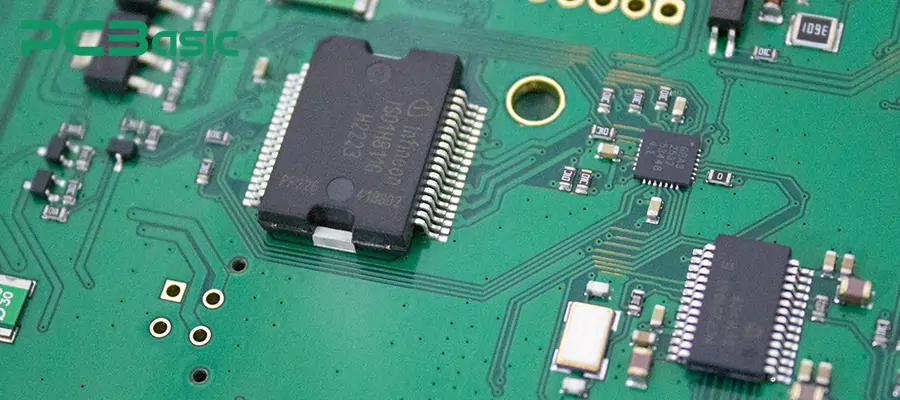
Although the assembly process is more complicated, engineers still choose 0201 components. This is because the advantages brought by the size of 0201 components cannot be replaced by other larger-sized SMD components. The specific reasons are as follows:
Firstly, there is an improvement in PCB density. By using 0201 type extremely small package components, designers can place more components within the same board area. Thus, they can achieve a higher level of functional integration without increasing the size of the PCB.
Secondly, the signal path will be shorter. Smaller device dimensions enable components to be placed closer to the chip, which helps to reduce parasitic inductance and parasitic capacitance.
In addition, the advantages of 0201 components in terms of size and weight also contribute to the creation of lighter and thinner end products. This makes them particularly suitable for applications such as smartphones, wearable devices, and compact IoT products that have strict requirements for structural dimensions.
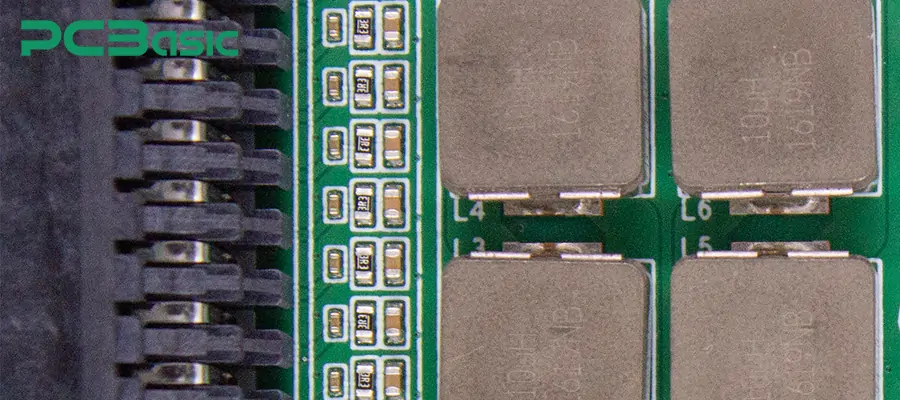
During the actual selection process, 0201 components are usually compared with 0402 package sizes. 0402 is widely regarded as a solution that achieves a good balance between size and manufacturability. Here is a comparison of 0201 and 0402 size components:
|
Feature |
0201 Component |
0402 Component |
|
Component Size (Metric) |
0.6 × 0.3 mm |
1.0 × 0.5 mm |
|
Component Size (Imperial) |
0.02″ × 0.01″ |
0.04″ × 0.02″ |
|
PCB Footprint & Layout Tolerance |
Extremely tight, strict DFM required |
Larger pads, more tolerant layout |
|
SMT Assembly Difficulty |
Very high |
Medium |
|
Defect & Yield Risk |
High if process is not optimized |
Low under standard SMT process |
|
Manufacturing Cost Impact |
Higher assembly cost |
Lower overall cost |
|
Typical Applications |
Smartphones, wearables, HDI modules |
General consumer & industrial electronics |
From a production perspective, 0201 has high costs and requires high yield rates. On the other hand, 0402 has stable assembly yields, is easier to inspect, and has lower rework risks. Therefore, when the PCB space permits, 0402 is usually the preferred choice.
During the PCB assembly process, the difficulty in using 0201 surface mount components is significantly greater than that of larger-sized SMD components. Assembly of components at this size level is highly sensitive to even minor process fluctuations, which can lead to defects or a decrease in yield. Common challenges in assembling 0201 components include:
1. The control of solder paste printing is very challenging.
Because the dimensions of 0201 components correspond to extremely small pads, the openings of the stencil are extremely fine. However, we also need to control the amount of solder paste printing with high precision. Even a slight excess or shortage of solder paste can cause problems such as bridging, insufficient wetting, or unstable solder joints.
2. The assembly accuracy must be extremely high.
Components of 0201 size require higher precision from the surface mount machine, as well as better visual alignment and repetitive positioning accuracy. Minor deviations that are acceptable on larger packages like 0402 or larger may cause component misalignment or incomplete soldering when applied to 0201 size.
3. Risk of tombstoning and component shift increases.
The smaller the solder joint volume, the more likely it is to be uneven due to heating and wetting. Therefore, the soldering of components with a 0201 package size is also a major challenge. During the reflow soldering process, proper design of the solder pads, temperature curves, or control of the solder paste quantity are all necessary; otherwise, tombstoning may occur.
4. The inspection difficulty has increased.
For the dimensions at the 0201 level, we cannot simply rely on visual inspection to meet the quality control requirements. We need to combine SPI, AOI to effectively identify any issues.
The above various factors indicate that not all PCB assembly factories have the ability to produce 0201 components stably.
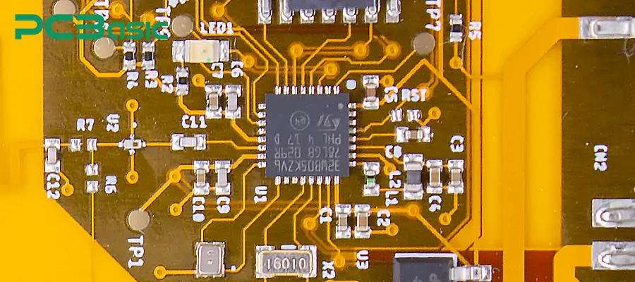
Components with the 0201 package size are often used in electronic products that have extremely strict requirements for size, weight and layout density. Common application scenarios include:
Smartphones and tablet devices
These applications have relatively high requirements for the integration of design. In such designs, 0201 components help to arrange more functional circuits within a limited space, meeting the demands of both slimness and high performance.
Wearable devices (such as smart watches and fitness trackers)
These products are extremely sensitive to PCB area and overall machine weight. Using SMD packages of size 0201 can significantly reduce the structural dimensions.
RF module and antenna-related circuits
In RF design, 0201 components can shorten the signal path and help reduce parasitic effects. This is of practical value for high-frequency performance.
Medical electronics and portable testing equipment
For small medical devices that have high requirements for size, reliability and integration, they often need to rely on ultra-small packaging to achieve functional integration.
High-density IoT and Embedded Systems
In modular and compact IoT designs, 0201 components can help the design achieve complex functional configurations within a limited board frame.
PCBasic possesses high-precision equipment, mature process control, and engineering experience specifically for micro-components. It can provide sample production and mass assembly services for 0201 package size components.
To ensure the assembly stability of the 0201 components, PCBasic will mainly control the following key aspects:
1. High-precision SMT assembly control. PCBasic ensures the accuracy and consistency of the assembly position while meeting the extremely small assembly tolerance requirements for 0201 components.
2. Stencil design and optimized solder paste printing. Through reasonable design of stencil apertures and control of solder paste printing parameters, the amount of solder is precisely managed, reducing common risks such as insufficient solder, solder bridging, and tombstone formation.
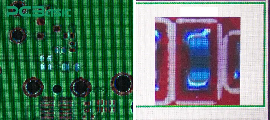
3. SPI, AOI and X-Ray inspection. Effective monitoring of solder paste printing quality, assembly status, and micro solder joints that are difficult to cover with manual inspection.
4. DFM engineering review before mass production. Before prototyping and mass production, evaluate the PCB layout and process plan to identify potential assembly and process risks in advance.
The 0201 components bring us numerous advantages, but they also come with obvious manufacturing challenges. Stricter pad tolerances, stricter solder paste printing control, higher assembly accuracy requirements, and more complex inspection methods all pose higher obstacles to PCB assembly. When choosing components, we cannot merely rely on their size. We should make the selection based on product size limitations, clear functional density requirements, and actual manufacturing capabilities.
Overall, when the design goals match the manufacturing capabilities, the 0201 package can play its due role in high-density PCB applications.
Time is money in your projects – and PCBasic gets it. PCBasic is a PCB assembly company that delivers fast, flawless results every time. Our comprehensive PCB assembly services include expert engineering support at every step, ensuring top quality in every board. As a leading PCB assembly manufacturer, we provide a one-stop solution that streamlines your supply chain. Partner with our advanced PCB prototype factory for quick turnarounds and superior results you can trust.

Assembly Enquiry
Instant Quote
Phone contact

+86-755-27218592
In addition, we've prepared a Help Center. We recommend checking it before reaching out, as your question and its answer may already be clearly explained there.
Wechat Support

In addition, we've prepared a Help Center. We recommend checking it before reaching out, as your question and its answer may already be clearly explained there.
WhatsApp Support

In addition, we've prepared a Help Center. We recommend checking it before reaching out, as your question and its answer may already be clearly explained there.