
Global high-mix volume high-speed PCBA manufacturer
9:00 -18:00, Mon. - Fri. (GMT+8)
9:00 -12:00, Sat. (GMT+8)
(Except Chinese public holidays)





HomePage > Blog > Knowledge Base > Wearable Medical Device PCB Assembly: From Miniaturization to Reliable Production
1. How Wearable Requirements Shape the Medical Device PCB
2. Manufacturing Risks in Miniaturized Wearable Medical PCB Assembly
3. Verifying Performance in Real Wearable Use
4. From a Working Prototype to Controlled Medical Production
Wearable medical device PCB assembly is not a simple process. For example, a health monitor is very different from a regular home device. A conventional electronic product may offer more room for PCB layout and component placement. In contrast, wearable medical devices often have tighter space constraints and more demanding quality and reliability requirements.
If a smart home device fails, it is annoying. If a medical monitor fails, a patient might get hurt. Therefore, strict steps must be followed to support product safety and quality.
This article discusses challenges and solutions in wearable medical device PCB assembly, with an emphasis on wearable medical devices. The shape of a PCB is of great importance and influences the final PCB assembly costs. Moreover, several tests are essential to ensure patient safety.
There are several considerations when designing a medical device PCB. One of the greatest challenges is the trade-off among a medical device's size, the functions it supports, and its battery life.
There are other physical constraints, e.g., component locations on a PCB and clearance rules between components. Often, a medical device PCB is populated with different functional components and integrated circuits that allow the device to perform its intended functions.
Nowadays, patients expect more from medical devices. For instance, some wearable medical devices may need to perform multiple sensing and monitoring functions. This could mean a device must integrate components to measure and transmit skin temperature, heart rate, and steps, to name but a few.
To maximize board space and minimize the size of a medical device, PCB designers use HDI boards. On an HDI board, laser drills are used to create connections between different layers of the board.
There is less space available on the top layer of the PCB if the wiring is not hidden. As a result, even fewer health sensors can be placed on the PCB. Keeping the wiring hidden is common in the design of medical wearable PCB assembly.
Also, PCB costs increase due to the small size of the components and the labor required to assemble the boards. The question is: is adding the extra feature worth the increased cost?
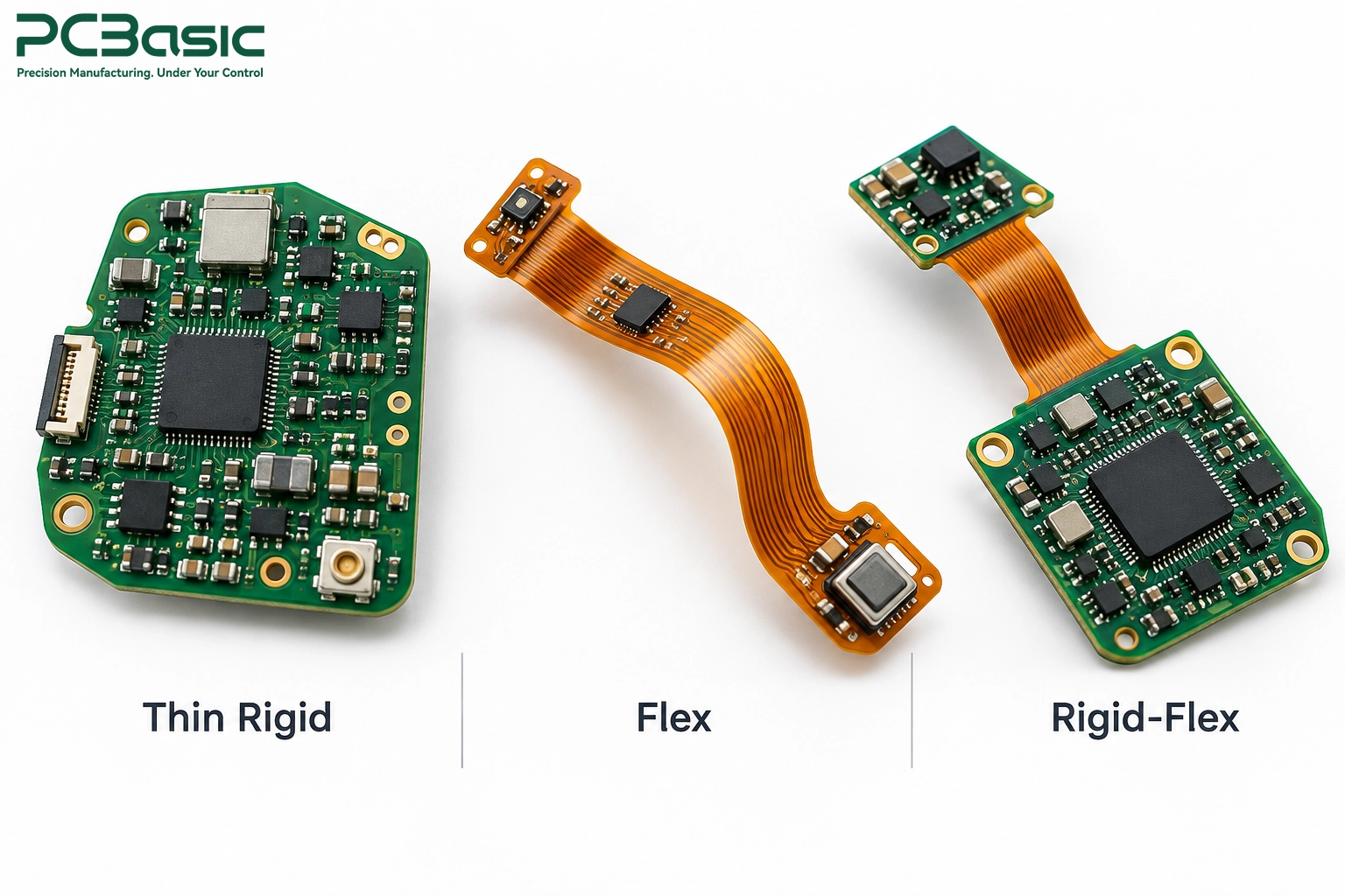
A PCB can't be shaped like a wrist and be expected to fit around the body's natural shape. A PCB design must be shaped to fit the body part it is intended to fit. There are 3 possible shapes for a PCB.
Thin, rigid PCBs are the most common boards used in wearables. They are used to make flat, triangular boards that electronics clip to a belt or vest. These boards are easy to manufacture and can withstand high heat. The main drawback of a thin, rigid board is that it can't be shaped to the body, unlike a board designed to be worn on the arm.
A bendable circuit board can easily conform to the arm's natural shape. A flex circuit can also take a lot of stress. Properly designed flex circuits can withstand repeated bending within their specified operating conditions.
Another option is a rigid-flex circuit, which combines rigid and flexible sections. A flex-rigid board can be designed to fit against the body, with a rigid section to hold a screen.
Rigid-flex boards are more challenging to manufacture than either fully flexible boards or rigid boards. A medical device manufacturer should assess the availability of special skills and equipment at a potential medical device contract manufacturing services (MDCMS) provider. The purpose is to ensure the provider can consistently assemble rigid-flex boards.
Power circuits can add noise and make the device less accurate. A well-thought-out and well-designed board can ensure that sensitive signals are not affected by noise and power circuits.
For a wearable medical PCB assembly, the optimal board layout can significantly improve the device's quality.
It is one thing to design and manufacture an electronic device in the lab. It is another to mass-produce the same device with incredible consistency. There are several hurdles to manufacturing small devices in volume.
Miniaturized assemblies require equipment and process settings capable of handling small components and tight placement tolerances. This is because the small components may get stuck in the equipment or fall off during assembly.
There are many processes in the manufacturing of small devices that require extensive controls and close supervision. This is especially true at the individual steps of the process, where things can easily go wrong. Below are the common problems and how to fix them.
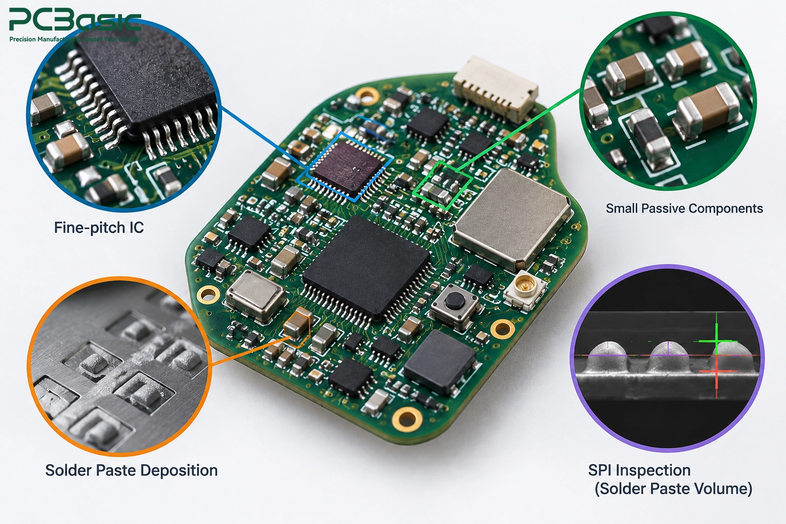
As stated earlier, the small components used in the manufacture of wearable medical device PCB assembly are smaller than a grain of sand. Standard SMT processes require tighter process controls when assembling such small components. One of the processes that requires close supervision is solder paste stencilling.
Stencil aperture dimensions and stencil thickness must be carefully controlled for very small components used in wearable medical device PCBAs. Small holes in the stencils quickly become blocked, thereby limiting the amount of solder paste transferred to the PCB. As a result, the components may not adhere well to the PCB or may fall off during assembly.
There are other problems associated with the placement of solder paste. At PCBasic, we have a strong capability in assembling 01005 and 0201 components. We use a Solder Paste Inspection (SPI) machine to assess the volume of solder paste to be applied to the PCB before components are mounted.
Old computer chips had metal legs on the edge that formed the circuit. One could examine whether the chips were manufactured and assembled correctly. Now, chips in medical devices are made differently.
These chips have internal connection circuits and cannot be examined by conventional means.
A bad connection under the chip cannot be seen, and it can make the whole board fail.
As mentioned above, X-ray inspection provides a non-destructive way to evaluate hidden solder joints and identify certain assembly defects.
A PCB may appear perfect and complete, but if the solder has not fully melted and formed a solid joint, the soldered joint will be weak and break under the slightest stress. In medical devices, PCBs must withstand shocks and vibrations.
It is hard to tell by eye whether the solder fully melted during reflow. To control the soldering process, we employ a strict thermal process and Automated Optical Inspection (AOI) to verify the presence of all components. For hidden solder joints, additional inspection methods such as X-ray may be used when required.
Evaluating the appearance of a prototype PCB is easy. Determining if that PCB performs its designed function is more difficult. Does the PCB in a wearable medical device accurately count the user’s heartbeats? Does a PCB in a wearable device reliably connect to a user’s cell phone via Bluetooth? You will not be able to answer these questions by simply looking at a PCB.
You must test the PCB in its designed environment. Functional testing PCBs prior to their enclosure being assembled provides an opportunity to avoid product waste. Furthermore, PCBA functional testing provides the customer with assurance that a quality product is being delivered.
Inspection of PCBAs is easy. It simply requires an optical comparison to a designed drawing. Functional testing of PCBAs is more difficult. It requires a system, software, and/or hardware to perform the required logic functions.
Some Original Equipment Manufacturers (OEMs) forego functional testing of PCBAs to reduce costs. A poor design decision: functionally defective PCBAs are permanently sealed inside a device and cannot be removed or replaced. This leads to wasted costs. It is more cost-effective to perform functional testing of PCBAs on the production line to catch defective ones.
It must endure extreme conditions. We test extensively. In-Circuit Testing (ICT) helps identify simple wire short circuits.
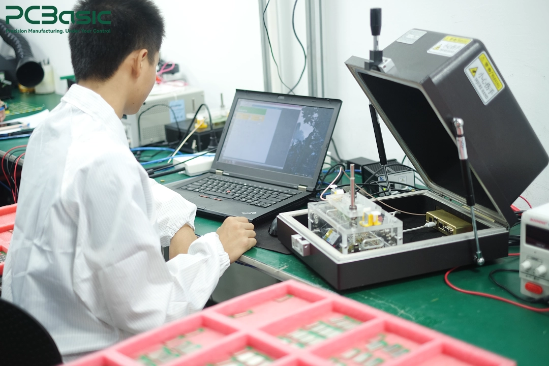
Functional Circuit Testing (FCT) is next. This test evaluates the complete functionality of the board. To perform this test, we develop test fixtures to simulate the function of the user interfaces and environments.
Additional testing is dependent on the specific end-use application of the board. If needed, we can subject the boards to a variety of environmental, temperature, and other stress tests.
Producing small quantities of boards in a lab is easy. Producing large quantities of boards in a manufacturing facility is very challenging.
Failures in a medical device can cause serious injury or death. Strict regulation and controls monitor the medical device industry. You must be able to substantiate and validate all the steps and procedures performed during the final assembly of the medical device.
Process uncertainty and variation must be identified, controlled, and reduced to acceptable levels. We will identify challenges and address issues that can occur during the mass production of a medical device.

In general, practices in the electronics industry allow for flexibility in bill-of-materials (BOM) management. For medical devices, strict control of all components is necessary. Supplier approval for medical device components is required.
You can’t let the factory make unilateral changes to parts. Engineers should review part changes. Even a small part change can alter how the device performs. You must maintain rules to protect patient safety.
Medical device makers must get the same result every time and be able to track every part. Let’s say you sell a medical device, and a memory chip in that device fails two years later. You need to identify the cause of the failure and correct it promptly.
Without part tracking, you may have to recall every device you made and could face lawsuits. This helps ensure patient safety and avoid potential legal liability.
Traceability means maintaining records that link the PCB assembly to relevant component lots, material batches, process records, inspection results, and test data. It is important in any failure; you can check which patients are at risk and take corrective action.
Your production system must be designed to ensure repeatability. At PCBasic, we utilize strict IQC on incoming raw materials.
FAI is performed on an initial assembly to verify that the product and manufacturing setup meet the specified requirements. Our MES system helps us track and trace every circuit board manufactured by the factory. This data supports manufacturing traceability and helps demonstrate conformance with applicable customer, quality-system, and product requirements.

Portable medical devices help patients and health practitioners by making it easier to monitor health conditions and medical data. While continuous advances in technology have enabled engineers to develop increasingly small devices, the miniaturization of medical electronics still poses several challenges, e.g., managing heat dissipation and mitigating mechanical failures in small components.
For the development of your next wearable medical device, PCBasic has the experience and manufacturing capabilities to support reliable wearable medical device PCB assembly in accordance with applicable customer and quality-system requirements.
Q1: What are the differences between a medical PCB and a consumer PCB?
Because of the risks associated with a failed product, e.g., a defective medical device, medical PCBs may require carefully selected materials, stricter process controls, and greater traceability during production to support the safety and reliability of the end product.
Q2: Why are flex PCBs so common in wearable devices?
Flexible PCBs can be designed to conform to the natural curves of the human body. In addition, flexible PCBs offer several advantages over rigid PCBs, e.g., they can be bent to conform to the natural curvature of a user’s arm or leg.
Q3: What is the hardest part about assembling tiny parts?
The most difficult aspect is placing the correct amount of solder paste on the circuit board. The components are extremely small. If the paste is applied incorrectly, the component will short-circuit or fall off during reflow.
Q4: Is X-ray inspection required for every wearable medical PCB assembly?
No. It is particularly useful for assemblies with hidden solder joints, depending on the component package and inspection requirements.

Assembly Enquiry
Instant Quote




Phone contact

+86-755-27218592
In addition, we've prepared a Help Center. We recommend checking it before reaching out, as your question and its answer may already be clearly explained there.
Wechat Support

In addition, we've prepared a Help Center. We recommend checking it before reaching out, as your question and its answer may already be clearly explained there.
WhatsApp Support

In addition, we've prepared a Help Center. We recommend checking it before reaching out, as your question and its answer may already be clearly explained there.
