
Global high-mix volume high-speed PCBA manufacturer
9:00 -18:00, Mon. - Fri. (GMT+8)
9:00 -12:00, Sat. (GMT+8)
(Except Chinese public holidays)





HomePage > Blog > Knowledge Base > How Are Consumer Electronics Trends Reshaping Flex PCB Assembly?
Table of Contents
1. Where Flex Assembly Risk Concentrates
2. What Consumer-Device Packaging Changes on the Shop Floor
3. Why Reflow and Handling Need a Different Support Plan
4. What Inspection Can Verify Before Motion Testing
5. How Motion Testing Defines Flex Durability
6. What the Supplier Must Receive Before Quoting
The flexible PCB assembly can pass the flat placement test, but they may not remain stable when integrated into the product. The real risks often occur after the board starts to bend, such as when passing through hinges, connecting flip screens, or moving repeatedly along with the product structure. Over time, problems like wiring cracking, solder pads lifting, poor connector contact, and even unstable signals or readings may arise.
Such problems usually do not occur randomly. We need to pay more attention to the transition areas between the flexible and rigid sections, stiffener edges, connector locations, and the areas that are repeatedly bent. These areas have more concentrated forces and are more likely to expose problems first.
Nowadays, consumer electronic devices are getting thinner and the connectors are getting smaller. A single flexible PCB assembly often needs to not only carry power, data, and sensor signals, but also move along with the product structure. Therefore, when assembling flexible PCBs, we cannot only consider whether the board can be adhered and whether it can pass the functional tests, but also need to figure out in advance: where will it move, and where must it remain flat. The subsequent support, assembly, and testing methods should all be arranged around these positions.
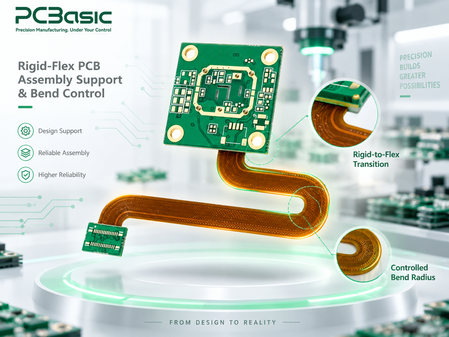
The assembly team needs more than a board outline. It needs to know the bend direction, bend radius, static or dynamic use, stiffener locations, connector keep-flat areas, and the expected movement in the finished product.
The bend zone should be treated as a controlled part of the process. Conductor position within the stack-up, copper thickness, coverlay construction, and layer symmetry influence how the material responds to bending. A radius that is fixed by the enclosure may leave little margin for manufacturing and assembly tolerances.
The buyer should provide the approved stack-up and identify the bend zones, not only describe them in a drawing note. The assembly team can then decide how to support the flexible material during printing, placement, reflow, depaneling, and inspection.
Stiffeners add rigidity near connectors, component pads, and handling areas, but the transition from flexible to rigid construction can concentrate stress if it is abrupt. The connector location, stiffener material and thickness, bend direction, and keep-flat area should be reviewed together.
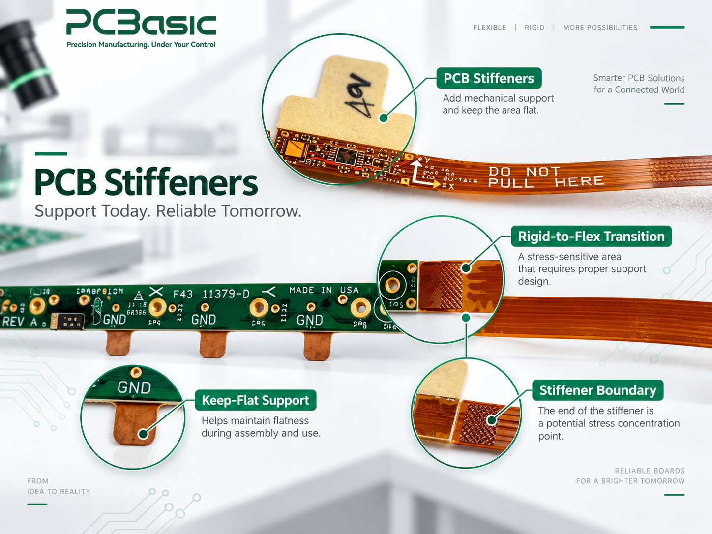
PCBasic supports rigid-flex PCB manufacturing with total layer counts up to 32 layers and FPC thickness starting from 0.08 mm. PI stiffeners are available from 0.05 mm depending on the application. Its Flex/Rigid-Flex inspection scope includes electrical test and design-rule checking. Those checks connect the stack-up and stiffener assumptions to an inspectable board construction, while the product's bend and acceptance conditions remain project-specific.
A static flex bends during installation and then stays in position. A dynamic flex continues to move during product use. The same stack-up may behave differently in the two cases because the accumulated strain and the number of movement events change.
The buyer should define the movement direction, the area that flexes, and the expected service condition before quotation. That information help determine how much process support and test evidence the project needs.
Smaller enclosures reduce the space available for carriers, tooling, and handling. A flexible circuit assembly may arrive as a panel, a supported strip, or a shaped circuit that cannot be processed like a rigid board. The physical format of the incoming assembly changes the production plan.
Connectors, test pads, and component clusters often need to stay flat while nearby sections bend. As the enclosure becomes smaller, those keep-flat areas can sit closer to the bend zone. Placement density increases at the same time, so the assembly team has less room for support features, tooling clearance, and inspection access.
The buyer should identify the keep-flat areas and the components that create them. That information allows the manufacturer to plan carrier geometry and handling before the first build.
One flex circuit may now carry power and data, connect multiple sensors, and accommodate mechanical movement. A single placement or connector defect can affect several product functions. The functional test should therefore reflect the actual signal and power paths, and the inspection plan should prioritize the features that carry more than one function.
This also changes the consequence of an approved substitution. A connector or stiffener change can affect mechanical fit, electrical or signal performance, and assembly support at the same time.
The carrier or support tooling should stabilize the flex during applicable processes such as solder-paste printing, placement, and reflow without loading sensitive bend or stiffener-transition areas. The panel design may need openings, relief areas, or support features that would not be required on a rigid board.
PCBasic's fixture scope includes SMT fixtures, wave-soldering fixtures, test fixtures, and soldering carriers. For a flexible circuit assembly project, the buyer should confirm which fixture is used, how it is identified, and how its revision connects to the flex release. A carrier that works for one product geometry may become a source of variation when the design changes.
Thin polyimide and adhesive layers can move, absorb moisture, or distort under heat. A process plan copied from a conventional rigid FR-4 board may not provide enough support for a flex assembly. The plan should describe how the flex enters the line, where it is supported, and how it leaves the process.
Moisture-sensitive materials and thin flex constructions may require controlled storage, preconditioning, or baking before reflow, depending on the material specification and exposure history. Heat can also create local movement around large stiffeners, connectors, or uneven copper areas. The process engineer should review component distribution, baking, and support requirements as one process plan.
The buyer should provide the approved material and stack-up so the production team can review thermal assumptions against the actual flexible construction.
A carrier or fixture keeps the assembly in a stable position while solder paste is printed and components are placed. For a flex board, the support plan should protect the bend region and maintain the connector keep-flat area. Unsupported movement can change paste deposition, placement accuracy, or connector alignment.
The carrier identification should be visible in the production record. If the carrier is revised, the change should be reviewed against the flex revision and the assembly result.
Depaneling and manual handling can introduce stress after the main assembly steps. PCBasic's production flow can include material baking, solder paste printing, SPI, placement, reflow, AOI, X-ray, wave soldering, depaneling, functional testing, and pre-shipment QA. The flex process plan should identify which of these steps applies and how the bend region is protected during each one. Some flex features have limited tolerance for repeated thermal or mechanical exposure.
A flex assembly service should explain how the bend region is protected between process steps and how an exception is recorded when rework is required.
Inspection coverage should follow the failure mode. AOI and X-ray answer questions about placement and solder conditions. They provide useful release evidence for the build, and they evaluate assembly quality before the product is subjected to repeated mechanical motion.
AOI can verify component presence, orientation, polarity, and visible solder conditions where the method is suitable. X-ray can inspect hidden solder joints when the board design and process plan justify it. Both methods should be tied to defined inspection points and acceptance criteria.
PCBasic's production controls include IQC incoming inspection, first-article approval, SPI, AOI, and X-ray. For a flex PCB assembly project, confirm which inspection points remain valid with the carrier and bend region, and record any method that requires a separate fixture or visual check. The inspection plan should state the limits of each method so the record does not imply broader coverage than the process provides.
The record should identify the flex revision, production lot, inspection stage, method, result, and disposition. If AOI or X-ray cannot verify a bend-related risk, the record should identify the separate test that covers it. This keeps each inspection record connected to the specific failure mode it is intended to detect.
Functional testing answers questions about electrical behavior under defined conditions. A dynamic flex application can require a motion or bend test that observes how the assembly behaves after repeated movement.
The functional-test specification should define the fixture, input conditions, power limits, test points, software version, and pass/fail thresholds. A board can pass an electrical test while lying flat and still fail after the product introduces mechanical movement. PCBasic supports functional testing and test-fixture development, and the agreed test specification determines what the result can prove for this product.
PCBasic supports functional testing and test-fixture development. MES and production records can connect the approved revision, incoming material, assembly operation, and test result when the project defines the identifiers to be retained. The buyer or product owner should define the motion test's acceptance criteria, while the manufacturing team confirms how the fixture and records will support it. The final record should connect the test condition to the flex revision and the production lot.
A flex PCBA quote is only as useful as its assumptions. The supplier needs enough design, mechanical, assembly, and test information to identify the process route and the evidence expected at release.
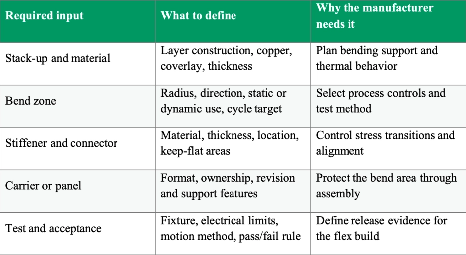
Provide the approved flex revision, material and thickness, layer construction, copper and coverlay details, bend direction, minimum / specified bend radius, and the area that can move. Static and dynamic requirements should be stated separately. If a bend radius is fixed by the enclosure, identify that constraint and the surrounding support geometry.
Identify the stiffener material and thickness, connector location, keep-flat area, and any handling region that requires extra support. Describe the panel or carrier format if it already exists, including ownership and revision. If the carrier will be designed by the manufacturer, state what geometry and inspection access must be preserved.
Define the functional-test fixture, electrical limits, software version, and pass/fail rule. For motion applications, add the bend or motion method, sample mounting, target cycle count, and measurement points. The accepted result should connect to the same flex revision and production lot.
A quote based on an incomplete stack-up or undefined test requirements can appear competitive while relying on assumptions that do not match the actual product. Reviewing those inputs first keeps the manufacturing proposal tied to the actual flex assembly.

In consumer electronics, the flexible PCB components require particular attention not to the entire board itself, but rather to a few more mechanically risky areas, such as the bending zones, stiffener edges, connector transitions, as well as the support methods of the board during reflow soldering and handling.
If these conditions can be clearly confirmed before the quotation and production, the assembly team can more reasonably arrange the support, handling and testing, and it will be easier to avoid problems that only emerge after the product is actually bent or moved in real use.
For rigid-flex PCB projects, it is also necessary to combine the approved stack-up, bending requirements and actual usage methods to confirm whether the manufacturing and testing plans are compatible. If you are preparing for a flex or rigid-flex PCB project, contact PCBasic with your Gerber files, BOM, bending requirements, carrier design and testing conditions, so that the key process details can be confirmed before production.
Q1: Why does a flex PCB fail near a stiffener or connector?
A1: Those transitions change the mechanical support around the bend. An abrupt or poorly located transition can concentrate stress and needs to be reviewed with the stack-up and bend direction.
Q2: What should a flex assembly quotation identify before pricing?
A2: It should identify the approved stack-up, bend zones, stiffener and connector details, carrier or panel format, component-placement constraints, and functional or motion-test requirements.
Q3: Can AOI and X-ray prove flex durability?
A3: No. They inspect placement and solder conditions. Bend life and motion behavior require the test method defined for the product and the approved acceptance limits.

Assembly Enquiry
Instant Quote




Phone contact

+86-755-27218592
In addition, we've prepared a Help Center. We recommend checking it before reaching out, as your question and its answer may already be clearly explained there.
Wechat Support

In addition, we've prepared a Help Center. We recommend checking it before reaching out, as your question and its answer may already be clearly explained there.
WhatsApp Support

In addition, we've prepared a Help Center. We recommend checking it before reaching out, as your question and its answer may already be clearly explained there.
