
Global high-mix volume high-speed PCBA manufacturer
9:00 -18:00, Mon. - Fri. (GMT+8)
9:00 -12:00, Sat. (GMT+8)
(Except Chinese public holidays)





HomePage > Blog > Knowledge Base > Surveillance Security PCB Assembly: A Complete Guide to Camera PCBs, Manufacturing, and Testing
Table of Contents
1. What Is a Surveillance Camera PCB and What Does It Control?
2. How Camera PCB Architecture Shapes Assembly Requirements
3. Manufacturing Challenges in Surveillance Security PCB Assembly
4. Surveillance PCB Assembly Process and Production Controls
5. Inspection and Functional Testing for CCTV and IP Camera PCBAs
6. Preparing a Surveillance Camera PCBA for Production
In
surveillance security PCB assembly, the choice of materials hinges on
functionality. Resistors, capacitors, sensors, processors, and copper, among
other parts, allow smart cameras to operate effectively even in the most
extreme operating conditions.
As demand for reliable surveillance systems grows, camera manufacturers place greater emphasis on consistent PCB assembly quality and long-term reliability.
However, the real question is how to assemble processors, sensors, power circuits, and communication components consistently. This complete process requires a high level of expertise and professionalism. A production defect can lead to camera failures or unstable performance in the field. Therefore, understanding the exact steps of surveillance security PCB assembly is completely necessary.
A camera PCB board is basically a core part of your security device. A camera PCB connects the image sensor, processing, power, and communication circuits. Depending on the camera architecture, processed video may then be transmitted through a wired or wireless interface.
But it is not necessary to overcomplicate how it works. You just need to know that a security camera circuit board does three basic functions:
1. It receives and distributes power from the camera's power source.
2. It processes the video data.
3. It supports video processing and communication through wired or wireless interfaces, depending on the camera design.
How do smart cameras effectively control electric power without adversely affecting the other components of the system? A CCTV camera PCB design has many small elements that work collaboratively. The main functions are:
1. It routes power for the screen, sensor, and motor.
2. Next, it processes images and turns raw signals into real pictures.
3. A camera PCB also communicates with storage so that it doesn’t get overloaded.
4. It also communicates with the other parts, mainly the lens, to carry out your instructions when the user presses the buttons several times.
5. It bridges connections like Wi-Fi or USB to send digital data to other devices.
At the same time, an IP camera PCB must process the digital data by compressing large video files in real time. Uncompressed video would crash a local network. It also runs motion-detection algorithms right on the silicon. Therefore, it saves a lot of bandwidth by only recording when someone actually walks past the lens.
In the market, you will see wide varieties of cameras. Subsequently, each variety comes with different types of PCB assemblies. So, what are the differences and which camera is suitable for what purpose enhances your knowledge.
|
Board Type |
What It Has |
Typical Use |
|
CCTV Camera |
• Video processing • IR / power control |
• Traditional CCTV systems • Coaxial video applications |
|
IP Camera |
• Image processor / memory • Ethernet interface |
• Network surveillance • NVR / server systems |
|
PoE Camera |
• PoE power circuit • Ethernet interface |
• Cameras using one cable for power and data |
|
Wireless Camera |
• Wi-Fi / RF module • Antenna interface |
• Installations where network cabling is limited |
Table: Comparison of CCTV, IP, PoE, and Wireless Camera PCBs
These categories can overlap. An IP camera may also support PoE or Wi-Fi, while a PTZ camera may add motor-control circuits.
Camera module PCB assembly is influenced by component density, package type, PCB structure, soldering requirements, and thermal characteristics. The board architecture therefore has a direct impact on assembly difficulty and process control.
Here, components are so densely packed that a PoE camera PCB assembly may use multilayer routing to accommodate power, high-speed data, and other camera circuits within limited board space. You have to keep high voltage away from delicate data streams. If you run a high-power trace right next to an audio trace, you will hear a constant humming noise on the microphone.
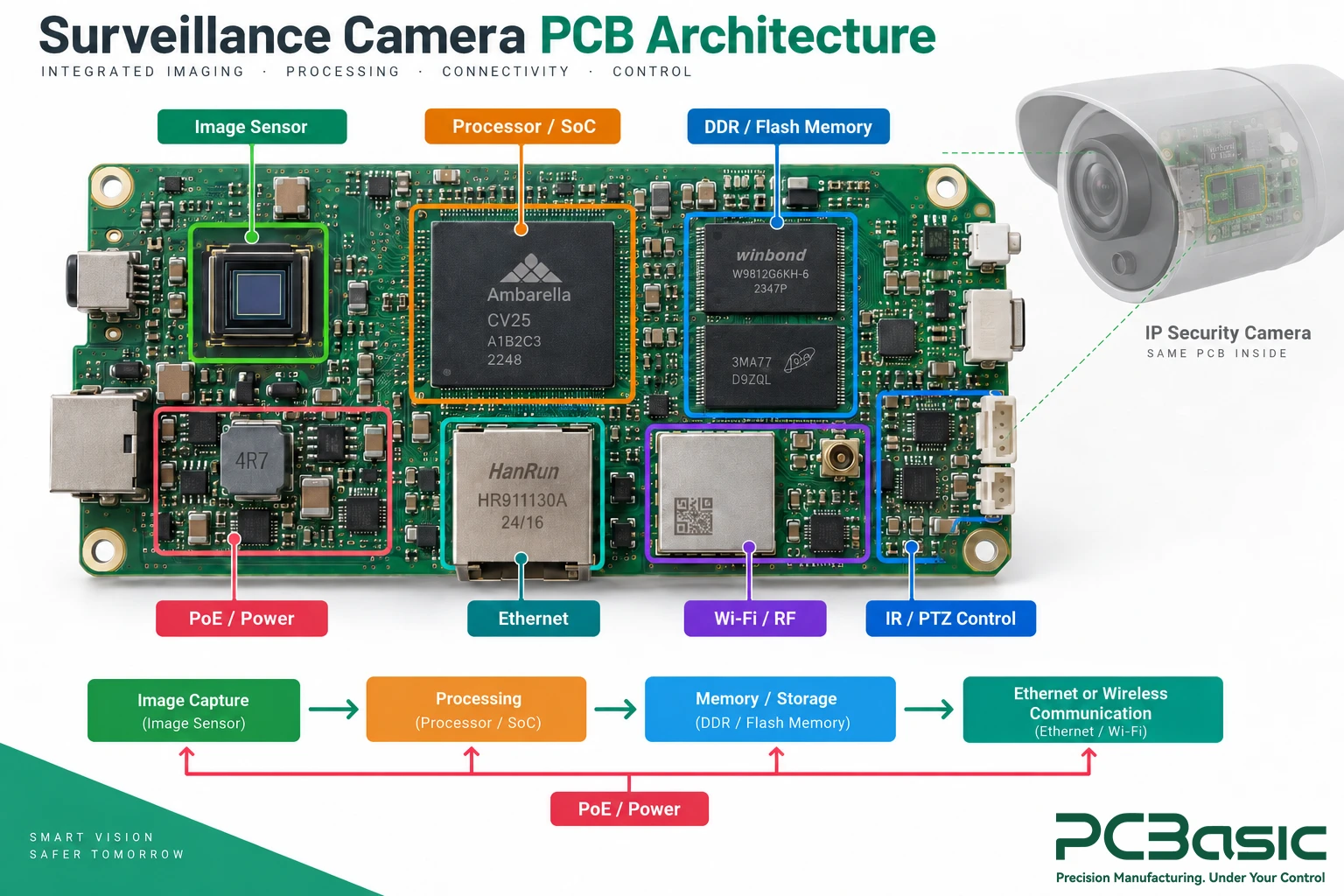
The performance of a focus-in camera is highly dependent on the image sensor, and positioning is tricky. Therefore, professional IP camera PCB assembly companies use pick-and-place machines to mount sensors at very tight tolerances. If the sensor tilts even a tiny fraction of a millimeter, the focus will be completely out on the left side of the video.
Outdoor cameras generally face very rigid environments, so their assembly also goes through a rigorous process. This is particularly concerning when their infrared lights turn on at night to see in the dark.
A PoE camera PCB assembly must manage power conversion and distribution while maintaining stable network operation. Power-over-Ethernet systems allow for high power to travel alongside sensitive network data.
There is a significant preference for device integration with reduced cable connections, and wireless cameras rank high on the preference list. A wireless camera PCBA completely relies on reliable radio frequency circuits.
Assembly defects around RF components, antenna connectors, or shielding can degrade wireless performance and cause unstable connectivity.
The use case for these products can be variable. Surveillance cameras may be deployed in indoor, outdoor, or industrial environments with different temperature and humidity conditions. If a PCB assembly contains a weak solder joint, repeated thermal cycling can increase the risk of intermittent or long-term failure.
Modern technologies are becoming virtually undetectable. New technologies and components are introducing hidden connections to modern products. For example, chips can have hidden joints beneath their plastic shell, with hundreds of pads/connections.
In the assembly of surveillance PCBs, these hidden solder joints cannot be inspected directly by visual inspection or conventional AOI, so X-Ray inspection may be used for BGA, QFN, and other bottom-terminated packages.
Supply-chain changes should not be handled by simply replacing components without reviewing the original and alternative datasheets. Even when two parts use the same package, differences in electrical characteristics, timing, thermal behavior, or firmware compatibility may affect camera performance. Substitutions involving memory, oscillators, power ICs, Ethernet PHYs, or wireless modules should therefore be reviewed before production.
Flux residue can contain moisture and cause premature PCB failure. This is true even if the solder joint is in good condition, as flux is essential during the soldering process.

It looks simple when you read that a camera PCB assembly goes through a solder paste printing, pick-and-place, and reflow soldering. However, if you are doing it for thousands of parts, you need a lot of discipline and skill. Therefore, PCBA companies do not compromise on strict factory controls at every single station.
Camera design precedes the mass production of all devices and saves time and money. Sample PCB assembly engineering teams execute a DFM analysis to verify compatibility. Example: Can all the parts fit within the available space on the printing surface?
The following stage is the Bill of Materials. A PCB assembly factory audits this as well and verifies that no chips will become obsolete very quickly.
For example, it is extremely embarrassing to have to redesign a printed circuit board because the only chip that fits within the specified cost limit is unavailable. This has a negative effect on your supply chain before you even start the major work.
Solder paste is printed through a metal stencil onto the PCB pads. Variations in paste volume, alignment, or stencil release can contribute to downstream soldering defects. Moreover, insufficient or excessive solder paste can create defects if it falls outside the validated process limits. PCBA companies use special cameras to scan the paste, which helps reduce operating costs and time.
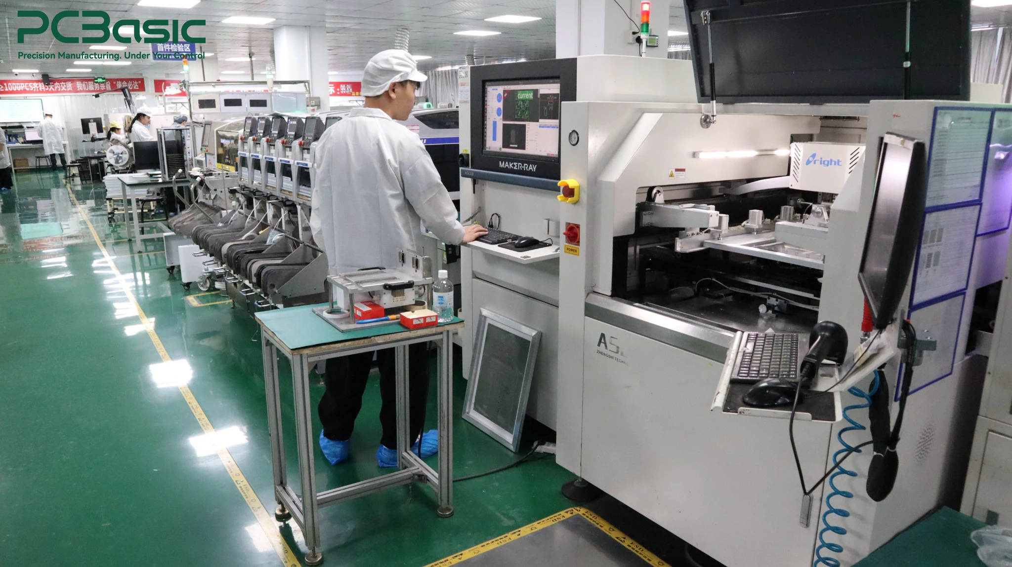
After reflow, the assembly may be cleaned when required by the flux chemistry, cleanliness specification, or subsequent processes such as conformal coating. Depending on the process, aqueous or other validated cleaning methods may be used.
A serial number or QR code may be laser-marked or otherwise applied to the PCB or assembly for traceability. Traceability records can help the manufacturer retrieve relevant production and material information for future builds, repairs, or failure analysis.
By scanning the barcode, the factory can determine which cassette was used in the assembly, the name of the operator who built the board, which PCBA build it was, and which solder batch was used to build it.
For surveillance camera projects, PCBasic combines DFM and BOM review, fine-pitch SMT assembly, SPI, AOI, X-Ray inspection, and production traceability. These controls help maintain consistent assembly quality from prototype and pilot builds through production, while processes such as cleaning or conformal coating can be applied according to product requirements.
You can't assume a board works just because it looks fine. Testing a CCTV PCBA involves three stages. Testing a CCTV PCBA usually combines structural inspection, electrical verification, and application-specific functional testing.
A proper IP camera PCBA test protocol identifies weak points early so you can fix them before shipping.
In PCBA, after you have applied the paste, the next stage is the inspection process. Here, 3D solder paste inspection systems measure solder paste height, area, position, and volume. This allows printing defects to be identified before component placement and reflow.
But after the oven, the Automated Optical Inspection machine begins its work. For example, it takes thousands of high-speed photos to check for missing chips and backwards parts.
The next step is electronic testing. In this testing, the PCBA team uses an In-Circuit Tester (ICT). ICT commonly uses a bed-of-nails fixture with spring-loaded probes that contact dedicated test points. The tester applies electrical signals and measurements to identify opens, shorts, incorrect component values, and other assembly faults.
At this stage, the electrical pulses provide useful information about whether a resistor's value is incorrect. They also allow inspection for an incorrect resistor value or a broken copper trace between layers.
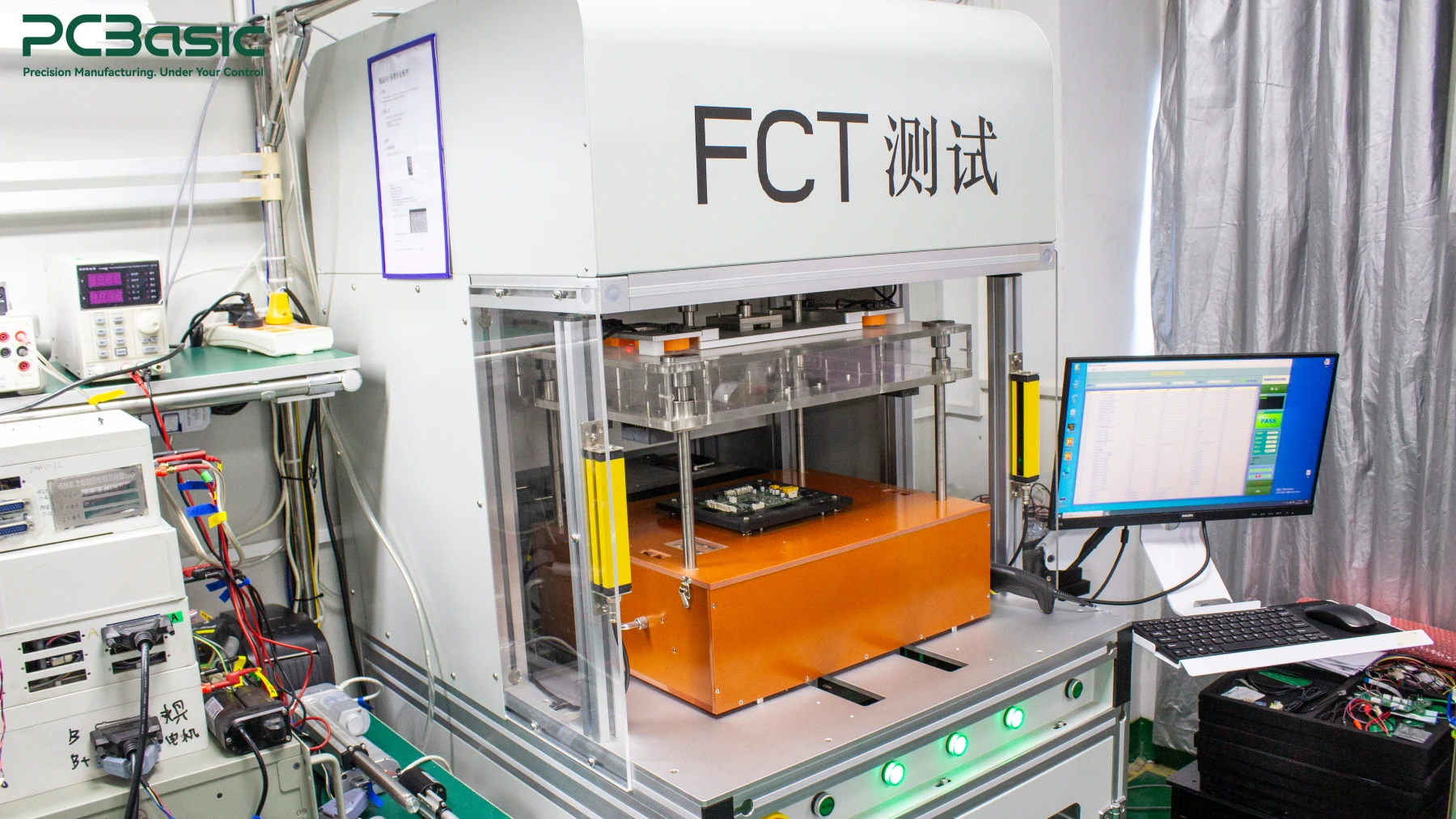
In this step, the board is powered up. Depending on the customer's test plan, the board may be programmed and installed in a dedicated fixture. Functional testing can then verify boot-up, image output, Ethernet or Wi-Fi communication, PoE operation, IR functions, storage, audio, or PTZ control where applicable.
Incomplete drawings sent to a PCBA factory result in an incomplete product. Security camera PCB assembly manufacturers require detailed instructions.
As a general example, machines will stop the line if instructions are incomplete. In your industry, disorganization can waste weeks of time.
The factory requires detailed Gerber files. These files show the factory where to place copper, green solder mask, and white silk screen. In addition, a detailed Bill of Materials Excel sheet is necessary.
Instructions on how to check the board are necessary. These details matter because they have no idea what the software can do. You need the final hex files or a flashing guide. It comes with instructions on which buttons to press.
Tell your manufacturer how you will use the camera, including the environment, so they can build a product that meets your conditions. Your manufacturer can also select the correct protective coatings and soldering profiles.
Lastly, define your burn-in testing requirements. This lets you specify exactly how many hours the boards bake in the heat chamber. As each hour spent in that chamber costs money, you must weigh up your need for reliability versus the cost.

A camera with better life and performance needs significant care in PCB assembly. Especially, reliable camera performance depends on both sound PCB design and consistent PCB assembly. The manufacturer must control materials, solder paste printing, placement, reflow, inspection, and functional testing so that the approved design can be reproduced consistently in production. So, you cannot rush manufacturing or skip the basic inspection steps.
Q1: Is it difficult to make surveillance security PCB assembly?
A1: Surveillance security PCB assembly includes many small assembly components. Therefore, a DIY approach is not an option. The answer is to contact a reputable PCB assembly company with the right tools and experience. This is very difficult because solder pads are extremely small, and it is easy to overshoot and damage the assembly.
Q2: Why do you need an X-ray machine to check camera circuit boards?
A2: X-ray machine can see the solder under the plastic, where regular cameras find it very difficult. An X-Ray inspection system can image solder joints hidden beneath packages such as BGAs and QFNs. It can help identify bridging, voiding, insufficient solder, and other hidden-joint abnormalities that cannot be inspected directly by conventional optical methods.
Q3: Do PoE boards need a different board layout?
A3: PoE circuits bring higher voltages directly onto the board. That means designers generally separate the chips’ high-voltage parts with high voltage from their sensitive data. This significantly reduces noise that can disturb video quality.
Q4: Can I actually scale a custom camera PCB design from a prototype to mass production?
A4: It is possible, but you need a good manufacturer to fix the design for mass assembly first. Scaling from prototype to mass production is possible, but the design, BOM, assembly process, test coverage, and production documentation should be reviewed and validated before volume production.

Assembly Enquiry
Instant Quote

Phone contact

+86-755-27218592
In addition, we've prepared a Help Center. We recommend checking it before reaching out, as your question and its answer may already be clearly explained there.
Wechat Support

In addition, we've prepared a Help Center. We recommend checking it before reaching out, as your question and its answer may already be clearly explained there.
WhatsApp Support

In addition, we've prepared a Help Center. We recommend checking it before reaching out, as your question and its answer may already be clearly explained there.
