
Global high-mix volume high-speed PCBA manufacturer
9:00 -18:00, Mon. - Fri. (GMT+8)
9:00 -12:00, Sat. (GMT+8)
(Except Chinese public holidays)





HomePage > Blog > Knowledge Base > How Heat and High Current Shape High-Power Charger PCB Assembly
1. Where Current Flows and Heat Builds Up
2. Soldering High-Current Terminals and Connectors
3. Mounting Power Devices to Heat Sinks
4. What Load Testing Reveals About the Assembly
When a power board carries tens or hundreds of
amps, the printed circuit board can act as a thermal bottleneck rather than a
simple interconnect. In high-power charger PCB assembly, electrical reliability
depends directly on how effectively the assembly moves current and sheds heat.
Consider a high-output charger power board built with heavy-copper traces, through-hole output terminals, and discrete power switches clamped to an external aluminum heat sink. For hardware engineers and procurement specialists, treating a high-power charger board like a conventional low-power PCB assembly can lead to cold solder joints, starved thermal pads, and stressed component leads. Every stage—from stencil design and selective soldering to mechanical fastening and electrical testing—must accommodate extreme thermal and electrical loads.
On a multi-kilowatt charger power stage, power conversion is never 100% efficient. Even a 96% efficient converter delivering 3.3 kW turns over 130 watts into waste heat inside a confined assembly.
Current enters at the primary input terminals, moves through the main conversion stages—such as input filtering, power factor correction, switching stages, isolation magnetics, or DC-DC rectification depending on the topology—and exits through heavy-duty output terminals. Along this path, resistive power loss (I2R) drives conduction heating. To manage losses and voltage drops, designs may specify increased heavy copper weights—such as 2 oz to 6 oz or thicker—alongside wide polygons and parallel internal planes.
During high-current PCB assembly, these thick copper planes aggressively pull heat away from localized soldering zones. Heavy copper boards may also use embedded copper coins for localized heat spreading, or busbars and thick jumper bars soldered onto the surface to supplement trace ampacity. Every transition point—component leads, vias, shunt resistors, and terminal blocks—introduces electrical resistance, linking solder joint integrity directly to electrical efficiency.
Most heat on a high-power charger PCBA originates at discrete focal points: power MOSFETs, rectifiers, magnetics, and current-sensing shunts. Heat travels from the silicon junction through the component package, across the solder joint or thermal interface material, into the PCB copper or an external aluminum heat sink, and out to the ambient air or cooling loop.
Designs rely on dense arrays of thermal vias beneath surface-mount power pads to pull heat to electrically compatible internal copper planes or bottom-side copper pours. If left open or improperly tented, molten solder can wick down these vias during reflow, starving the thermal pad and creating voids. Excessive voiding beneath a power package can act as a thermal barrier, raising junction temperatures and potentially accelerating thermal fatigue.

While surface-mount components handle control and switching, heavy power enters and exits through plated through-hole terminals, screw lugs, blade connectors, and busbar tabs. Achieving a sound metallurgical bond on these soldered interconnects is a core challenge in charger PCB assembly (by contrast, press-fit pins rely on mechanical interference in plated holes rather than solder metallurgy and require dedicated pressing tooling).
Standard wave or hand-soldering profiles may require adjustment when a heavy terminal pin enters multiple layers of 4 oz copper. Even with thermal relief spokes—which engineers must balance against current-carrying capacity—the surrounding copper acts as a massive heat sink.
If the soldering iron tip or selective nozzle cannot deliver heat faster than the copper conducts it away, solder fails to wet the barrel walls, causing cold joints or insufficient vertical fill. Assembly houses prevent this without scorching laminates or lifting pads by using:
• High-thermal-capacity selective soldering: Programmable selective nozzles extend dwell times on heavy power and ground pins while controlling nitrogen shrouding and underside preheat.
• Controlled board preheating: Raising bulk PCB temperature evenly before soldering narrows the thermal delta, allowing solder to flow through plated holes without excessive tip temperatures.
• Custom step stencils for pin-in-paste: When reflow-compatible high-current headers undergo reflow with SMT parts, stepped stencils deposit extra paste locally around through-hole apertures to support adequate barrel fill and fillet formation.
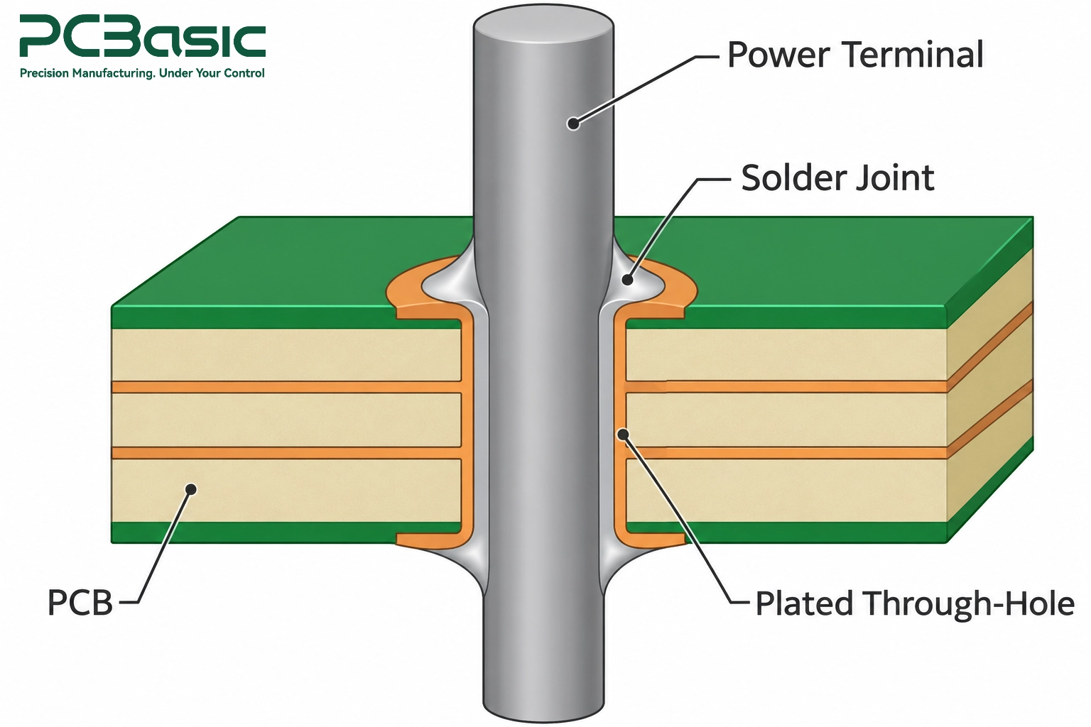
A connector sitting crooked or raised off the board can introduce mechanical leverage and uneven stress on its solder joints. When a user mates a heavy charging cable, an unintended gap between the connector housing and PCB can transfer mechanical stress directly into the solder fillets.
Visual inspection alone is insufficient for heavy power connectors. Automated Optical Inspection (AOI) checks visible fillet geometry and connector seating, while 2D or 3D X-ray inspection may be used during first-article inspection (FAI) and batch audits to evaluate internal barrel fill in thick multilayer boards. Acceptable vertical solder fill is judged against the IPC-A-610 class and customer drawing requirements specified for the project—particularly where large thermal mass or terminal geometries dictate distinct fill criteria—while also checking for proper wetting and unacceptable blowholes caused by moisture or other sources of outgassing in thick laminates.
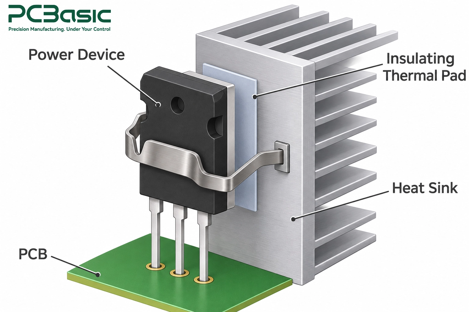
In high-wattage chargers, through-hole power packages—such as TO-220, TO-247, and TO-264 MOSFETs or rectifiers—are typically mounted vertically along the board edge and clamped directly to an extruded aluminum heat sink or metal chassis. Subtle process errors at this mechanical-electrical interface cause major field failures.
Because most power transistor metal tabs are electrically live (typically tied to the drain or collector), they must be electrically isolated from a grounded heat sink while maintaining low thermal resistance. Depending on voltage isolation and mechanical tolerances, assemblers use electrically insulating thermal interface pads, polyimide films with thermal grease, or ceramic insulators like alumina and aluminum nitride (non-insulating phase-change materials or thermal greases alone are only suitable when electrical isolation at that interface is not required or is provided by the package itself). For specific package footprints, creepage distances, and hole clearances, process engineers cross-check vendor application notes—such as Mounting Considerations for Power Semiconductors—against the assembly drawing.

Minor flaws at this interface create immediate reliability risks:
• Contamination and debris: A stray solder ball, hard contaminant, or metal burr trapped between the transistor tab and an insulating pad can puncture soft silicone under clamping pressure, causing dielectric breakdown or a chassis short during high-potential (Hi-Pot) testing.
• Misalignment and incomplete coverage: If an insulating pad shifts during hardware installation or fails to provide the specified coverage around the tab edges, creepage and clearance distances may be compromised, increasing the risk of electrical breakdown.
• Grease inconsistency: When thermal compound is paired with a thin film or ceramic wafer, the application process must maintain uniform thickness; too little can leave air voids, while too much can increase thermal resistance and cause squeeze-out.
Never pull an already-soldered power package flush against a heat sink by tightening its mounting screw afterward. If an assembler solders a TO-247 MOSFET first and then cranks down a screw to close a mechanical gap, the rigid copper leads act as levers, locking mechanical tension into the solder joints and package. Subsequent thermal cycling in service can crack the solder fillets or damage internal package interconnections.
To prevent residual lead stress, production teams may mount devices to the heat sink or an alignment fixture before soldering, in accordance with the package manufacturer’s instructions:
1. Power devices are inserted into the unsoldered PCB and aligned flush against the heat sink (or a proxy fixture) with thermal interface materials and insulating shoulder washers in place.
2. Fasteners are secured per engineering specs—screws are tightened with calibrated torque drivers to specified torque values, while spring clips are seated into retention slots so the thermal interface compresses evenly without cracking ceramic insulators or over-stressing the package.
3. Once mechanical position is locked, leads are soldered via selective or wave soldering, allowing joints to solidify without excessive mechanical preload.
AOI and X-ray confirm physical workmanship, but power electronics require electrical stress to verify assembly integrity under operating conditions. Charger load testing bridges structural inspection and field deployment by driving defined current through the power stage before shipment.
Using programmable electronic loads and separate Kelvin voltage-sensing connections, test engineers measure voltage drop across critical power interconnects and sensing elements—such as DC busbar joints, current-sensing shunts, and charging output terminal connections—at specified steady-state currents. Even a few milliohms of unexpected resistance appear as a measurable voltage deviation under high current.
When an interconnect exhibits a voltage drop outside the baseline window, technicians perform targeted troubleshooting: inspecting the affected terminal or busbar joint for incomplete barrel fill, checking connector mating surfaces for oxidation or poor seating, and verifying fastener torque on bolted lugs. Catching abnormal voltage drops at end-of-line testing prevents localized resistive heating from degrading board materials in service.
Thermal profiling during burn-in or extended load testing validates mechanical and thermal assembly steps. Test stations pair infrared (IR) thermal cameras or thermocouples with defined load profiles until the assembly reaches a specified stabilization point.
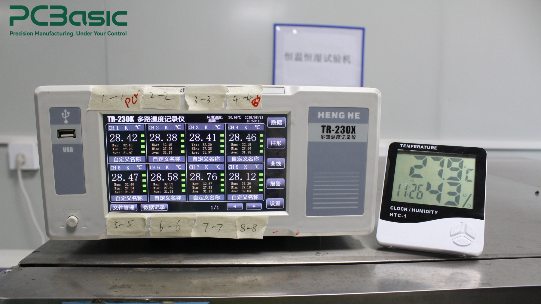
Thermal measurements under load flag assembly anomalies that look normal at room temperature. If two identical parallel MOSFETs sharing the same gate drive and power nodes show an unexpected temperature split under steady load, engineers inspect that specific device location—checking fastener torque or clip seating, verifying thermal pad placement and thickness, or reviewing X-ray images for solder voiding beneath the package where a soldered thermal pad is present. Localized heating at an output terminal block likewise prompts a closer look at through-hole wetting and terminal seating.
In high-power charger PCB assembly, electrical performance and thermal management are locked together. Heavy copper demands tailored preheat and selective soldering profiles; high-current connectors require strict seating checks; and heat-sink-mounted semiconductors depend on stress-free mounting sequences and clean thermal interfaces.
Sharing complete mechanical and test documentation up front can reduce time spent on line debugging. You can submit your BOM, Gerber files, heat sink assembly drawings, thermal interface specifications, and load-test criteria directly to PCBasic—a full-service PCB and PCBA manufacturer offering free DFM review, heavy-copper capability, functional testing, and burn-in services—for an assembly quote.
Q1: What information does the assembler need for heat sink mounting and load testing?
The assembly partner needs mechanical assembly drawings showing fastener types and torque specs, part numbers or thickness tolerances for thermal pads and electrical insulators, Hi-Pot test parameters, and a load-testing procedure specifying test points, current levels, duration, and pass/fail voltage-drop or temperature limits.
Q2: Should power transistors be soldered before or after mounting them to a heat sink?
Power devices should never be pulled flush against a heat sink by tightening screws after their leads are soldered. In many through-hole assembly workflows, devices are aligned and fastened to the heat sink (or an alignment fixture) first so leads are soldered without locked-in mechanical stress, subject to the package manufacturer's instructions.
Q3: What defects can charger load testing help identify that AOI and X-ray miss?
While AOI and X-ray inspect physical geometry, charger load testing evaluates functional electrical and thermal behavior under real current stress. It can flag high-resistance interconnects through abnormal voltage drops, and it can help identify uneven heat sink contact, misplaced thermal pads, or excessive solder voiding in soldered thermal pads through localized temperature rises under sustained load.

Assembly Enquiry
Instant Quote


Phone contact

+86-755-27218592
In addition, we've prepared a Help Center. We recommend checking it before reaching out, as your question and its answer may already be clearly explained there.
Wechat Support

In addition, we've prepared a Help Center. We recommend checking it before reaching out, as your question and its answer may already be clearly explained there.
WhatsApp Support

In addition, we've prepared a Help Center. We recommend checking it before reaching out, as your question and its answer may already be clearly explained there.
