
Global high-mix volume high-speed PCBA manufacturer
9:00 -18:00, Mon. - Fri. (GMT+8)
9:00 -12:00, Sat. (GMT+8)
(Except Chinese public holidays)





HomePage > Blog > Knowledge Base > Complex PCB Assembly Services: What to Check Before Choosing a Manufacturer
1. What Makes a PCB Assembly Project Complex?
2. Can the Manufacturer Handle Your Board’s Requirements?
3. How Will Assembly Quality Be Verified?
4. What to Confirm Before Starting a Complex PCB Assembly Project?
For purchasing managers and lead engineers alike, sourcing complex PCB assembly services is rarely a routine transactional exercise. It is a high-stakes vetting process. A misstep at this stage can mean delayed product launches, failed field tests, and wasted engineering hours.
When dealing with advanced electronics—whether for medical devices, aerospace, automotive systems, or high-reliability industrial IoT—contract manufacturers without the necessary process capabilities may struggle to meet your requirements. You need a partner with specialized equipment, rigorous process controls, and deep engineering intuition. This guide breaks down what engineers and procurement teams must evaluate before handing over their design files to a complex PCB assembly manufacturer.
Complexity in electronics manufacturing isn’t defined by a single metric. Rather, it is a cumulative burden of tight tolerances, advanced packaging, and unforgiving material behaviors.
An 0805 resistor is no longer a useful benchmark for fine-pitch assembly capability. Today’s high-density designs may feature 01005 (imperial designation) passive components, flip-chips, and ball grid arrays (BGAs) with pitch sizes dropping below 0.4 mm. Handling complex PCB assembly requires precise alignment systems and process control. Placement errors relative to the component pitch and pad geometry can cause bridging between adjacent BGA solder joints or misaligned passives, resulting in electrical faults or intermittent failures that are notoriously difficult to debug.
Designs utilizing High-Density Interconnect (HDI), microvias, stacked vias, blind/buried vias, and rigid-flex substrates introduce unique thermal and mechanical stresses. During reflow soldering, materials expand at different rates. If copper thickness, bare-board quality, moisture absorption, and thermal exposure conditions are not properly evaluated alongside the oven's thermal profile, issues like substrate delamination or barrel plating cracks can compromise reliability.
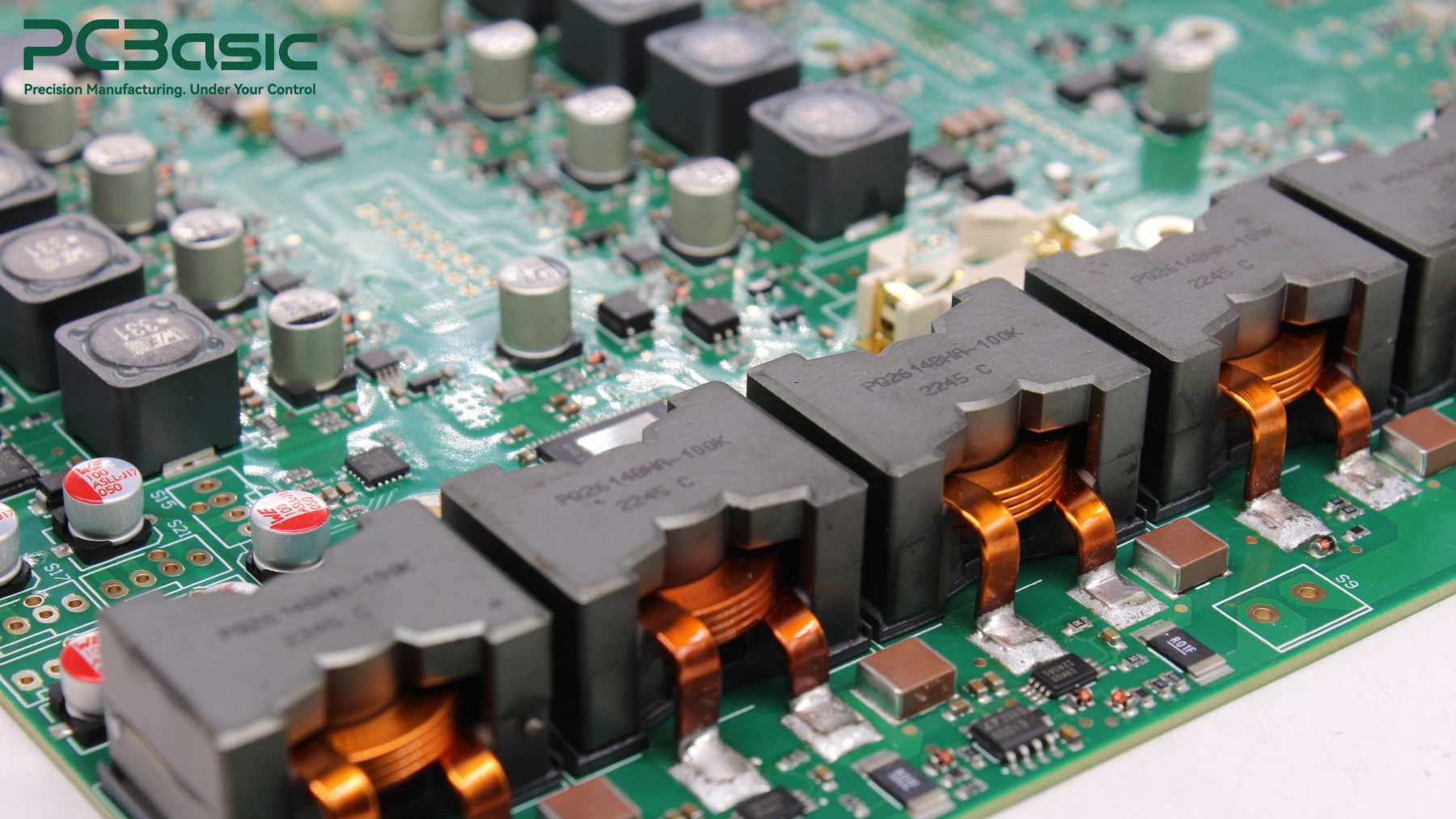
High-power industrial boards often combine heavy copper layers (3 oz or more) with delicate surface-mount components. Solder joint formation becomes challenging because heavy copper planes act as thermal sinks, drawing heat away from the soldering zone. Balancing these thermal profiles demands process engineering expertise. Furthermore, when designs combine high-density SMT with selective through-hole components, coordinating wave soldering, selective soldering, or hand-assembly steps requires precise process sequencing.
Ultimately, managing high-complexity PCB assembly means controlling dozens of variables simultaneously. If your manufacturer lacks the process discipline or engineering experience to anticipate these challenges, your project can stall on the production line.
Evaluating a potential manufacturing partner requires looking past marketing brochures and examining their actual shop floor capabilities and engineering workflows. Engineers and procurement professionals should evaluate three key operational areas:
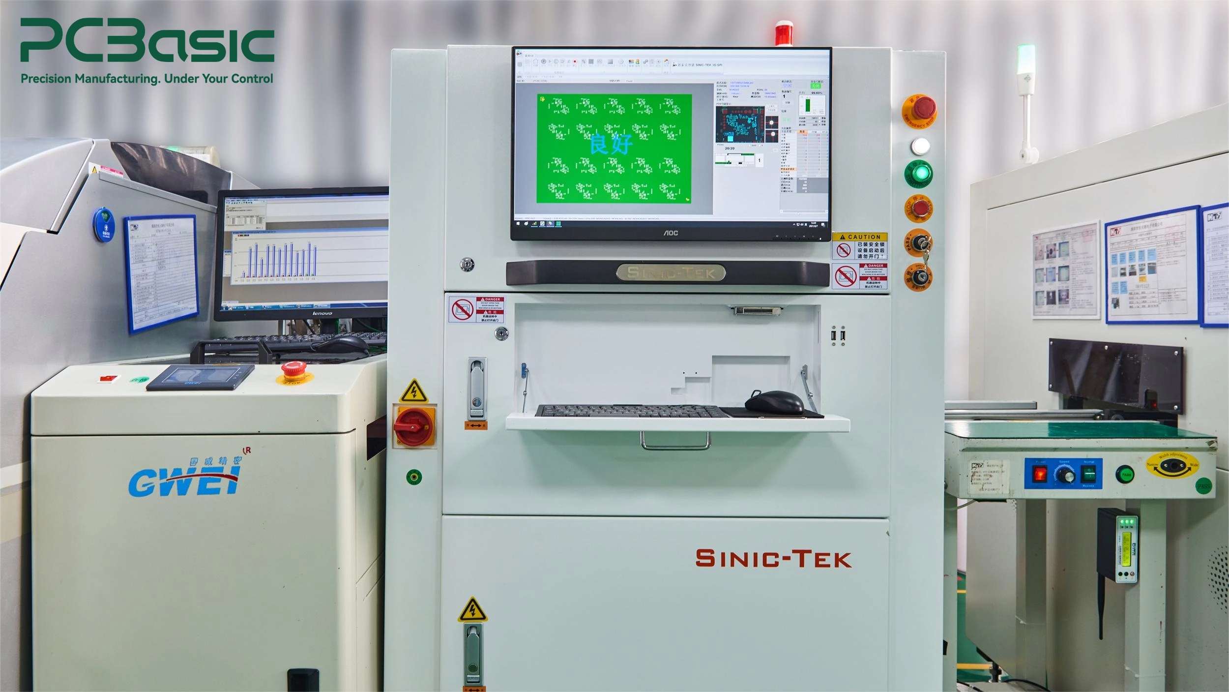
Review the manufacturer's placement machinery, solder paste printing technology, and inspection systems. Rather than searching for an arbitrary precision number, confirm whether their placement equipment and process controls meet the exact tolerance and pitch requirements of your specific component package mix. Advanced 3D Solder Paste Inspection (SPI) directly after printing is highly valuable—catching paste volume variations or printing offsets before component placement protects yields downstream.
A capable assembly partner reviews your design files systematically before production. When you request complex PCB assembly services, the vendor's engineering team should provide a clear review summary detailing:
• Scope of the manufacturing review performed;
• Identified thermal relief, pad geometry, or clearance risks;
• Any unresolved engineering queries requiring design adjustment.
A smooth review with no major changes required does not automatically indicate a lack of scrutiny; what matters is transparency regarding what was checked and verified.
Quality management system certifications like ISO 9001, AS9100, ISO 13485, or IATF 16949 should be verified for validity, scope, and coverage of the manufacturing site based on your product’s target industry and applicable customer and regulatory requirements. Rather than comparing simple layer counts, evaluate a manufacturer’s track record with similar packaging constraints, thermal challenges, and test requirements.
At PCBasic, projects are matched with dedicated engineering oversight and tailored production workflows. By integrating 3D SPI, automated optical inspection, X-ray inspection, and flexible electrical testing solutions (such as flying probe or custom ICT/FCT setups), PCBasic aligns shop-floor equipment and process controls directly with your specific design complexity.
Quality must be engineered into the process from solder paste deposition through final testing. Because modern electronics feature hidden solder connections beneath BGAs, CSPs, and QFNs, visible inspection alone cannot confirm joint integrity. A comprehensive quality plan uses complementary inspection and testing methods.
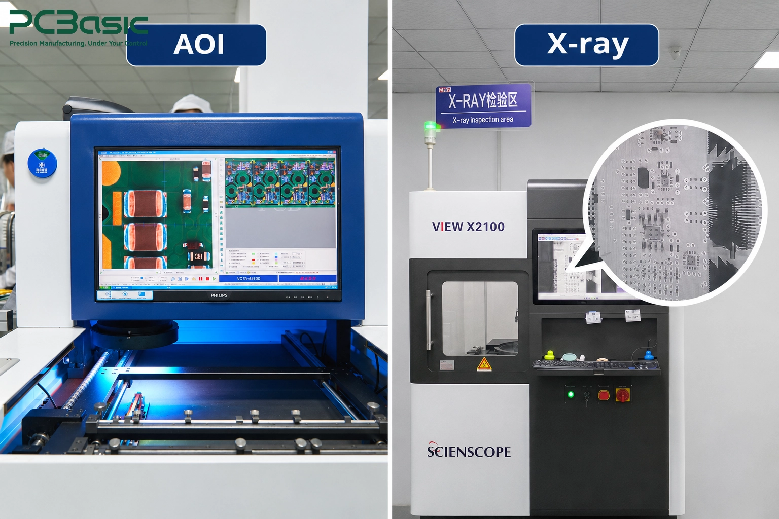
Visual inspection and Automated Optical Inspection (AOI) remain valuable for verifying visible component presence, orientation, polarity markings, and surface fillet quality. However, for array packages and hidden joints, X-ray inspection is used to analyze internal solder structure, detect voiding, and identify indications of soldering defects underneath component bodies. Neither tool replaces the other; they provide complementary coverage of failure modes across the assembly.
Beyond visual and X-ray checks, electrical performance must be verified based on design testability and access points:
• In-Circuit Testing (ICT): Checks for shorts, opens, and passive component values using dedicated pin fixtures, subject to test access and circuit limitations.
• Flying Probe Testing: Offers flexible electrical structural verification without requiring custom bed-of-nails tooling—ideal for prototypes and low-to-medium volume builds.
• Custom Functional Testing (FCT): Powers the board under operating conditions to run diagnostic firmware or functional validation routines.
To ensure clear alignment on quality standards, both parties should confirm the verification plan and applicable acceptance criteria, including the agreed IPC class and customer-specific requirements, prior to production:
• Inspection Coverage: Define which assemblies or components undergo sample inspection versus 100% inspection across SPI, AOI, and X-ray stations.
• Functional Test Scope: Document test inputs, operating conditions, interface connections, and explicit pass/fail criteria.
• Quality Records & Retest Rules: Establish how test logs are recorded and define mandatory re-inspection/re-test protocols for any reworked components.

Moving a complex build into production requires closing the gap between engineering documentation and commercial agreements.
Counterfeit components present a major risk to advanced electronics. When evaluating turnkey PCB assembly services, verify the manufacturer’s component procurement channels. Confirm whether parts are sourced through franchised distributors or original component manufacturers, and verify that clear lot control and date-code traceability are maintained throughout storage and handling.
Prior to job release, perform a complete audit to align all production files. The Bill of Materials (BOM), Gerber/ODB++ files, pick-and-place XY coordinates, and mechanical assembly drawings must reflect the same approved product configuration. Mismatches between BOM part numbers and footprint patterns can cause pre-production delays.
Ensure your quotation explicitly details all commercial elements. Clarify costs for NPI setup, stencils, ICT/FCT test fixture fabrication, test software development, and specialized process steps (such as conformal coating or underfill).
Tie target lead times to concrete project milestones: receipt of complete engineering files, file approval, material kit staging, and first-article inspection approval. True schedule predictability depends on full material readiness and signed-off documentation before line setup begins.
Protecting intellectual property is essential. Ensure formal Non-Disclosure Agreements (NDAs) are signed, and confirm that data transfer protocols for your schematics and layout files meet agreed security requirements.

Navigating advanced electronics manufacturing requires clear technical alignment, thorough process verification, and transparent commercial agreements. By evaluating potential partners based on equipment match, DFM review clarity, inspection coverage, and supply chain control, you reduce avoidable manufacturing risks and improve delivery predictability.
Whether you are scaling a medical diagnostic system, an automotive controller, or a high-performance compute module, choosing an experienced partner for complex PCB assembly services helps turn potential production hurdles into a more controllable, repeatable process.
If you are preparing your next high-density design for production, contact PCBasic today. Submit your Gerber files, BOM, assembly drawings, and testing specifications to receive a comprehensive engineering review and transparent manufacturing proposal tailored to your project.
Q1: What is the difference between standard PCB assembly and complex PCB assembly?
Standard assembly typically involves traditional surface-mount and through-hole components with standard spacing and lower density. Complex PCB assembly typically involves high-density packaging (such as fine-pitch BGAs, CSPs, or 01005 passives), advanced board structures (like HDI or rigid-flex), heavy copper thermal considerations, or multi-step soldering workflows that require tighter process control.
Q2: Why should I consider turnkey PCB assembly services for a high-complexity build?
Opting for turnkey assembly consolidates board fabrication, component procurement, assembly, and testing under a unified management process. While turnkey services do not guarantee shorter lead times for all component supply scenarios—and may involve specialized sub-contracted processes—they simplify project coordination, assign single-point operational accountability, and streamline engineering communications.
Q3: Is running an automated EDA rule check sufficient to ensure my board is ready for assembly?
Automated DRC/DFM checks in EDA software are essential first steps, but they do not replace a full manufacturing review. Factory reviews evaluate component clearances against specific SMT line capabilities, stencil design rules, thermal requirements for reflow, and actual inspection/testing accessibility.
Q4: Is X-ray inspection required for every high-complexity PCB assembly?
X-ray inspection is primarily used to evaluate hidden solder connections, such as BGA balls, QFN ground pads, or bottom-terminated components, where optical inspection cannot see the joint. The extent of X-ray inspection—whether 100% inspection or sampling—should be decided based on your specific component packaging, product reliability requirements, and agreed test plan.

Assembly Enquiry
Instant Quote

Phone contact

+86-755-27218592
In addition, we've prepared a Help Center. We recommend checking it before reaching out, as your question and its answer may already be clearly explained there.
Wechat Support

In addition, we've prepared a Help Center. We recommend checking it before reaching out, as your question and its answer may already be clearly explained there.
WhatsApp Support

In addition, we've prepared a Help Center. We recommend checking it before reaching out, as your question and its answer may already be clearly explained there.
