Table of Contents
1.What Is an Automated Optical Inspection Machine in PCB Assembly?
2.Manual Visual Inspection vs. Automated Optical Inspection
3.Where AOI Fits in the SMT Production Line
4.How an Automated Optical Inspection Machine Works
5.Common PCB Assembly Defects Detected by AOI
6.Key AOI Machine Parameters Buyers Should Understand
7.AOI vs. SPI, X-Ray, ICT, and FCT
8.What Buyers Should Ask Before Choosing a PCBA Manufacturer with AOI
9.PCBasic's Approach to AOI in Small and Medium Batch PCBA
10.FAQ
Each component on a printed circuit board (PCB) must be placed precisely. Using the wrong resistor, overlooking a cold solder joint, or allowing component misalignment beyond the specified tolerance can lead to higher field failure rates, more costly rework, or even product recalls. As PCBs become more complex and the pitch density of their components increases, it has become impossible to detect defects reliably through manual inspection alone.
The solution to this problem is Automated Optical Inspection (AOI).
AOI machines have quietly become one of the most critical components in
today's surface mount technology (SMT) assembly lines, and while AOI machines
may not be the most visible component of the overall manufacturing process,
they provide rapid, consistent, and highly repeatable inspection results that
considerably exceed the results obtained by manual inspections of high-volume
production runs.
This guide will explain how AOI systems detect defects; what types of
defects they can and cannot detect; the operating parameters that may result in
leaving certain types of defects undetected; and what questions buyers should
consider before evaluating the quality control systems offered by a PCBA
supplier.
What Is an Automated Optical Inspection Machine in PCB Assembly?
AOI Meaning in SMT and PCBA Manufacturing
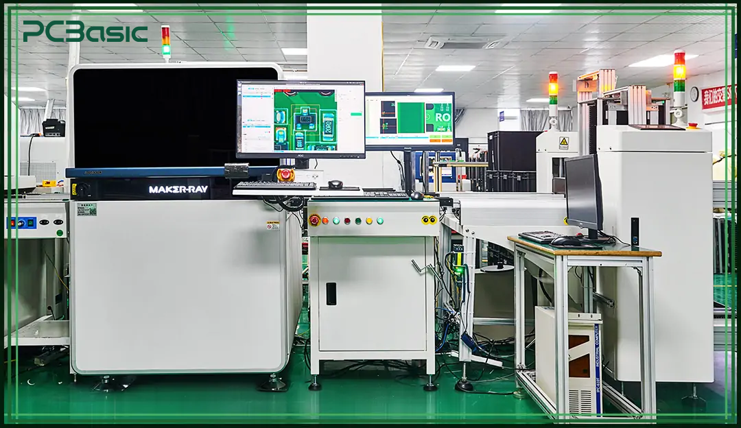
Automated
Optical Inspection (AOI) is an automated method used to inspect a populated
Printed Circuit Board (PCB) through high-resolution cameras and structured
lighting. The system compares captured images of the PCB against a reference
standard and flags any discrepancies.
AOI
machines are typically placed at key stages in the production line. They are
commonly positioned either immediately after component placement or after
reflow soldering, with each location serving a different purpose in detecting
defects as early as possible.
AOI
technology is referred to in different ways, including Automated Visual
Inspection (AVI) or Optical Inspection Systems. Regardless of the terminology
used, all these terms describe the same automated inspection technology used in
modern PCB manufacturing.
Manual Visual Inspection vs. Automated Optical Inspection
The
practice of manual visual inspection (MVI) has been a part of the electronics
industry since the first PCBs were assembled. A trained inspector uses a loupe
or a magnifying glass to examine a board for defects or potential defects. This
is quite effective for simple boards populated with large through-hole
components; however, modern-day surface-mount technology (SMT) boards pose a
challenge.
Components
like 0201 passives, fine pitch ball grid arrays (BGAs), and quad flat no-leads
(QFNs) require a specific level of magnification, lighting, and focal length,
which are difficult to maintain over the course of an eight-hour shift.
Additionally, the human inspector experiences fatigue and as a result, the
defect escape rates significantly increase after the first two hours of
inspection, and again, increase during the fifth hour. This is not a reflection
upon individual capabilities, but rather an indication of how visual attention
works during repetitive tasks.
Conversely,
Automated Optical Inspection (AOI) does not suffer from these effects. The
machine utilizes the same algorithm to evaluate both board number 1 and board
number 5,000. The lighting is the same, the camera's position does not move,
and the evaluation criteria do not change throughout the production run.

Where AOI Fits in the SMT Production Line
Most
SMT lines place AOI at two key points: after component placement and after
reflow soldering.
Post-placement AOI is used before the board
enters the reflow oven. At this stage, the AOI machine checks whether
components are missing, shifted, rotated, or incorrectly oriented. This helps
catch placement problems before solder joints are formed.
Post-reflow AOI is the most common
AOI position. After the boards exit the reflow oven and solder joints have
formed, the AOI machine scans for visible soldering defects, placement errors,
missing components, tombstoning, solder bridges, and polarity issues. This is
the primary quality gate in many SMT production environments.
Some high-complexity lines add a
second AOI pass after selective soldering or wave soldering for through-hole
components. The specific placement depends on board complexity, defect history,
and production volume.
How an Automated Optical Inspection Machine Works
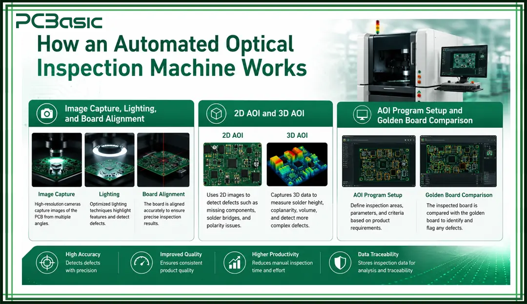
Image Capture, Lighting, and Board Alignment
The
alignment of a circuit board will occur after it is loaded into an Automated
Optical Inspection (AOI) machine. The position of the PCB is determined by a
set of small reference or fiducial marks that the AOI uses for reference. An
offset alignment will render all comparisons invalid.
After
the alignment process is complete, the AOI machine uses a camera or multiple
cameras (depending on the size of the PCB) mounted above the circuit board to
capture images of the PCB in defined sections, or Fields Of View (FOVs). The
quality of the image can greatly depend on the lighting used. Most AOI machines
in use today have installed multi-color, multi-angle LED lighting to create
shadows that give a visual indication of solder joint shape and finish, as well
as component height and finish. In 3D AOI systems, the quality of the images is
further enhanced using structured light patterns, which provide exact vertical
measurements of the component height in addition to the visual information.
2D AOI and 3D AOI
2D
Automatic Optical Inspection (AOI) utilizes two-dimensional imaging to examine
the boards from directly above, capturing the image in a flat plane. The
purpose of 2D AOI is to verify that components are present, properly
positioned, and polarity is correct, along with verifying the basic appearance
of the solder joint. In addition, the 2D version of AOI is very fast and
cost-effective. Most types of standard printed circuit boards will have most of
the defects detected using 2D AOI inspection systems.
3D
Automated Optical Inspection (AOI) adds the third dimension to the board
inspection by not only acquiring the images of the solder joints in a flat
plane, but also creating a height map of the image of the solder joint and the
component. This addition of height information to the inspection results in
additional defect detection, as some defects are very obvious in the height
data, although they were not detectable in the 2D or flat image. Some defects
that require 3D characterization to detect include see-sawed leads,
insufficient volume of solder at the joint, and slight warpage.
In
summary, 3D Automated Optical Inspection (AOI) provides very different
capabilities from 2D Automated Optical Inspection. There is also a significant
price differential with 3D AOI systems costing significantly more, often two to
three times more, than the equivalent 2D AOI system for comparable production
volumes.
AOI Program Setup and Golden Board Comparison
Every
AOI machine needs a program before it can inspect a new board design. Two main
approaches exist. The first is CAD-based programming, where Gerber files, BOM
data, and centroid files are imported directly. The second is golden board
teaching, where a verified, defect-free board is scanned, and the machine
learns from that image set.
Both
methods have tradeoffs. CAD-based programming is faster to set up for new
designs. Golden board methods can be more accurate for boards with unusual
finishes or special components, but they depend entirely on the golden board
actually being defect-free, which isn't always guaranteed.
Common PCB Assembly Defects Detected by AOI
Component Placement Defects
The
automated optical inspection system is particularly good at catching placement
problems. Common defects it detects include:
• Missing components
— the pad is there, the component isn't
• Skewed or rotated
components exceeding programmed angular tolerance
• Wrong polarity on
capacitors, diodes, and ICs
• Tombstoning — where
one end of a passive component lifts during reflow
• Shifted components
where placement offset exceeds pad overlap limits
Soldering Defects
AOI
can provide a very useful function in detecting solder bridges, which are a
dangerous defect that occurs when excess solder connects two pads that should
NOT be connected when viewed from above. AOI will typically be able to detect
solder bridges when the bridge is in plain view from above.
When
insufficient solder has been applied to the component, the resulting solder
fillet will be small in size or not have adequate pad 'wetting' that allows the
solder to properly adhere to the pad. Solder balls, flux residue patterns and
cold joints (which can often be identified through dullness and/or roughness)
are also within the detection capability of the AOI system.
Surface and Marking Defects
Beyond
placement and soldering, AOI also flags PCB-level issues: damaged pads, missing
silkscreen markings, lifted traces near component edges, and incorrect
component labeling when character recognition is enabled.
Defects AOI Cannot Fully Detect
It's
worth being honest about the limitations. AOI sees the surface. It cannot see
inside a solder joint, under a BGA package, or into a via. Voids in BGA solder
balls, a common reliability concern, are invisible to optical inspection.
Shorts beneath low-clearance packages, open joints under QFNs, and any defect
hidden by the component body itself require X-ray inspection. Functional
defects, such as wrong component value, incorrect IC programming, and marginal
parametric performance, are outside AOI's scope entirely.

Key AOI Machine Parameters Buyers Should Understand
Camera Pixels, Pixel Resolution, and FOV
Camera
resolution determines how small a defect the machine can reliably detect.
Resolution is typically expressed in microns per pixel; the smaller the number,
the finer the detail visible. For inspecting 0201 components and fine-pitch ICs
with 0.4mm or 0.5mm lead pitch, you generally need resolution in the 10–15
micron range.
PCB Size, Thickness, Clearance, and Warpage
Every
automated optical inspection machine has a maximum board size it can handle.
Common limits run from around 50×50mm minimum up to 510×460mm or larger for
panels. Warpage tolerance is an often-overlooked spec. A maximum of 1–2mm is
typical; heavily warped boards need fixturing or simply won't inspect reliably.
Inspection Speed and Production Fit
Inspection
speed is usually quoted in cm²/second or boards per hour for a reference board
size. Match the machine's throughput to your line speed, not just the spec
sheet. An AOI machine that takes twice as long as your reflow oven creates a
bottleneck.
Typical AOI Parameter Examples
|
Parameter
|
Typical Range
|
|
Camera Resolution
|
8–20 µm/pixel
|
|
Max PCB Size
|
510 × 460 mm
|
|
Min PCB Thickness
|
0.5 mm
|
|
Max PCB Warpage
|
≤
1.5 mm
|
|
Inspection Speed
|
60–150 cm²/sec
|
|
Repeat Accuracy
|
±15 µm or better
|
AOI vs. SPI, X-Ray, ICT, and FCT
AOI vs. SPI
SPI
(Solder Paste Inspection) checks paste volume, area, height, and offset before
any components are placed. SPI catches paste printing errors early, before the
cost of components is involved. AOI post-reflow catches the results of
everything that happened after paste printing. The two systems are
complementary, not interchangeable.
AOI vs. X-Ray Inspection
X-ray
inspection is the tool for seeing what AOI can't. BGAs, QFNs, CSPs — any
package where the solder joints hide underneath need X-ray to verify joint
quality. AOI is faster and cheaper per board; X-ray is slower and more
expensive, but reveals what optical systems physically cannot see.
AOI vs. ICT and FCT
In-Circuit Testing (ICT) uses a bed-of-nails
fixture to probe individual nodes and verify component values, shorts, and
opens. Functional Circuit Testing (FCT) powers up the board and tests it like a
real device. In a well-designed quality program, AOI, ICT, and FCT all
complement each other, each catching what the others miss.
What Buyers Should Ask Before Choosing a PCBA Manufacturer with AOI
Is AOI Inline or Offline?
Inline
AOI connects directly to the SMT conveyor; boards pass through automatically
without manual handling. Offline AOI requires operators to load boards by hand.
"We have AOI" and "we have inline AOI" are meaningfully
different answers. Ask specifically.
How Are AOI Programs Created and Verified?
A
poorly configured AOI program is almost worse than no program, it generates massive false alarm rates,
operators start accepting callouts without reviewing them, and real defects
slip through. Ask how programs are created, how tolerances are set, and how
often programs are audited and updated.
How Are AOI Defects Recorded and Traced?
For
every error flagged by a machine, you should create a record consisting of the
defect type, the location on the PCB, the time and date of the error, the
machine ID, and the status (or disposition). All this data will build into a
picture of where your defects are being created (which processes are drifting)
and where you're seeing yield loss overall. If a manufacturer is able to give
you defect trend reports, then they are using their AOI information correctly.
How Does AOI Work with Rework and Final Inspection?
AOI
is a detection tool, not a fix. Boards with confirmed defects need rework. Ask
how rework is authorized, documented, and re-inspected. A board that went
through rework should have that history attached to its traveler record. Final
inspection should happen after any rework, not before.
About PCBasic
Time is money in your projects – and PCBasic gets it. PCBasic is a PCB assembly company that delivers fast, flawless results every time. Our comprehensive PCB assembly services include expert engineering support at every step, ensuring top quality in every board. As a leading PCB assembly manufacturer, we provide a one-stop solution that streamlines your supply chain. Partner with our advanced PCB prototype factory for quick turnarounds and superior results you can trust.
PCBasic's Approach to AOI in Small and Medium Batch PCBA
At PCBasic, AOI inspection is applied to both SMT and DIP assembly. In the SMT process, 8 VCTA-A480 SMT AOI inspection systems are used after reflow soldering to check visible defects such as missing parts, component offset, polarity errors, tombstoning, solder bridges, and poor solder joint appearance. In the DIP process, PCBasic uses a DIP AOI inspection system from Leichen Technology to inspect plug-in components after insertion and soldering.
For small and medium batch PCBA projects, this separation is important. SMT AOI focuses on dense surface-mount components, while DIP AOI helps control the quality of through-hole components, connectors, and other plug-in parts. Together, they make AOI more suitable for mixed-technology PCB assemblies rather than only standard SMT boards.
AOI in the SMT Quality Control Flow
Post-reflow AOI provides fast feedback after soldering. If several boards show the same solder bridge on the same component, the issue may be related to solder paste volume, stencil aperture design, placement accuracy, or reflow settings. Finding this repeated pattern early helps engineers adjust the process before the defect affects more boards in the batch.
Flexible AOI Use for Multi-Variety Small-Batch Projects
High-mix,
low-volume PCBA is where AOI program management becomes a real discipline.
Switching between ten different board designs in a single shift means ten
different inspection programs need to be accurate and ready. Libraries of
reference data, standardized tolerance templates by component family, and
version-controlled program files make this manageable.
Combining AOI with Other Inspection and Testing Methods
A
practical quality system for medium-complexity PCBA typically layers solder
paste inspection (for print quality), post-reflow AOI (for placement and
soldering), X-ray sampling (for BGA and hidden-joint verification), and
functional testing (for electrical verification). AOI is the highest-throughput
layer; it processes every board quickly. The other methods catch what AOI
misses, at their respective cost and time tradeoffs.
Conclusion
Modern
PCBA manufacturers require an automated optical inspection machine as the
base-level expectation for any production environment that prioritizes quality.
However, no single inspection system can detect every defect. That is why a
properly programmed AOI system, when integrating into the reflow stage,
provides one of the most efficient quality checks for surface-visible defects,
placement accuracy, and solder joint appearance.
If
you are evaluating potential PCBA suppliers, asking "Do you have an AOI
machine?" is not the right question to ask. Rather, you should be asking
how the AOI machine fits into the overall quality flow, how programs are
updated to meet changing production requirements, and how defect data from the
AOI is used to enhance the overall process. The information you receive in
response to these questions will ultimately provide you with a better
understanding of a manufacturer's culture of quality than what one could get
simply by looking at the specifications on the AOI machine.
If
you are searching for a 3D AOI machine for your facility or evaluating contract
manufacturers, a better understanding of what AOI can and cannot do will give
you the information necessary to make a good decision.
FAQ
Q: What is AOI in PCB assembly?
AOI
(Automated Optical Inspection) is a machine-based system that uses cameras and
lighting to scan PCBs for defects such as missing components, solder bridges,
misalignment, and polarity errors by comparing them to a reference standard.
Q: What is the difference between 2D and 3D AOI?
2D
AOI uses top-down images to detect visible surface defects. 3D AOI adds height
measurement using structured light, allowing detection of issues like
insufficient solder or lifted leads that are not clear in 2D images.
Q: What defects can AOI not detect?
AOI
cannot inspect inside solder joints or beneath components. Defects like BGA
voids, hidden shorts, or electrical faults require X-ray or functional testing.
Q: How much does an automated optical inspection machine cost?
Prices
vary by system type. Basic 2D offline systems start around $30,000–$60,000,
inline 2D systems range from $80,000–$150,000, and advanced 3D systems can
exceed $200,000–$400,000 depending on features.
Q: Is AOI the same as SPI?
No.
SPI checks solder paste before placement, while AOI inspects components after
placement or reflow. They are different but complementary processes.
Q: What should I ask an AOI-equipped PCBA manufacturer?
Ask whether AOI is
inline or offline, how inspection programs are created, how defect data is
used, and how reworked boards are verified. These details matter more than just
having the machine.