Global high-mix volume high-speed PCBA manufacturer
9:00 -18:00, Mon. - Fri. (GMT+8)
9:00 -12:00, Sat. (GMT+8)
(Except Chinese public holidays)
Global high-mix volume high-speed PCBA manufacturer
9:00 -18:00, Mon. - Fri. (GMT+8)
9:00 -12:00, Sat. (GMT+8)
(Except Chinese public holidays)
HomePage > Blog > Knowledge Base > What is Silkscreen PCB? A Beginner's Guide
Silkscreen PCB, commonly called legend printing, is an additional layer used to construct a printed circuit board (PCB) that refers to surface printing of text, symbols, and graphics. This layer has many purposes: It gives fundamental data for the PCB assembly, testing, and usage.
Electricians make a silkscreen with a non-electrically conducting epoxy ink. It is usually used on the component side of the PCB. Some components and test point identifiers, warning signs, and other branding information are usual items in the silkscreen process. Without this information, putting together and identifying a problem in a PCB is a daunting task, particularly in circumstances where there are multi-layered boards.
This guide article discusses what silkscreen is, the type of silkscreen used in the manufacturing of PCBA, the symbol used, and check methods. At the end of the article, you will understand what role silkscreen PCB plays in the current electronics manufacturing industry and how it helps to enhance the quality and performance of PCBs.
Silkscreen on PCB serves multiple critical functions in the assembly process:
Ensures Accurate Installation: Different labels and symbols on the PCB silkscreen help the technicians accurately identify the placement of several components so that the correct assembly is done. And they can aid in minimizing mistakes throughout the assembly process through proper labeling of the parts.
Improves Production Efficiency: Silkscreen on PCB offers a way of showing some components of the design by pointing, thus reducing the time required to assemble diagrams.
Avoids Assembly Errors: In silk screening there is information labeled as component designations, polarized marks, and directions. If the information is not right positioned, then it can lead to the wrong connection.
Facilitates Testing and Debugging: Using the right silkscreen on PCB enables the technicians to follow test points for a circuit and to debug if there are any in the future. This makes the testing to be faster and more efficient.
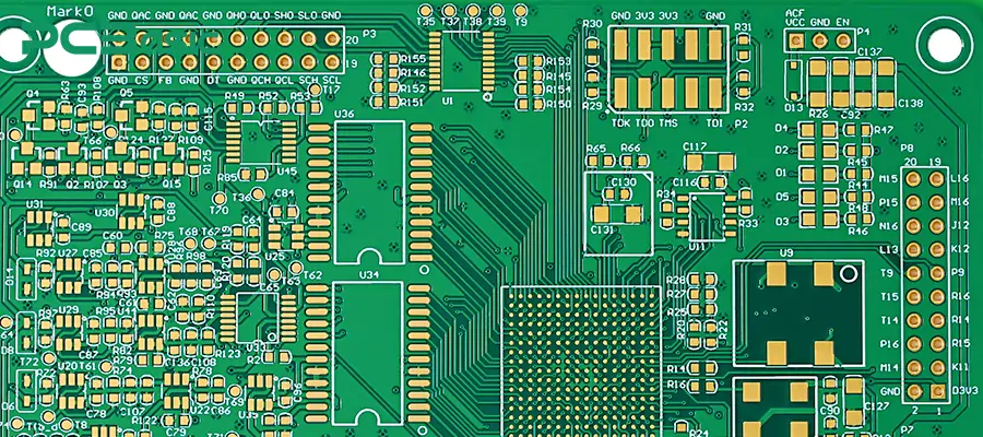
There are several types of silkscreen PCB used in PCBA manufacturing, each serving different purposes depending on the design and requirements of the board:
Top Silkscreen: It is the most frequently used silk screen on the top layer of PCBs and is used to add text or graphics to a PCB. It has tags for the parts, identification symbols, and other marks that are useful in a construction and inspection sequences. Top silkscreen is most relevant to single-sided PCBs or boards where most components are mounted on only one side.
Bottom Silkscreen: Sometimes, components are also placed on the bottom side of the PCB and, therefore, bottom silkscreen is required. This layer is similar to the top silkscreen layer and contains the labels and marks of the components to be assembled at the back of the board.
Edge Silkscreen: Edge silkscreen is ink printed on the outside of the PCB along the border and is mainly used to guide PCBs assembly. It may also incorporate branding data, like logo and board version, which is helpful for recognizing and tracking.
Indicator Silkscreen: Some PCBs possess special indicators such as arrows, symbols, or LEDs to indicate the status of certain board parts. For instance, a power indication silkscreen might only give users feedback that the board is on or off.
Pin Number Silkscreen: This type of silkscreen indicates PINs on Integrated Circuits and Connectors to indicate their orientation and placement. It is important to refer to pins correctly, especially when it concerns multi-pin components, which may lead to major circuit problems as a result of wrong pin alignment.
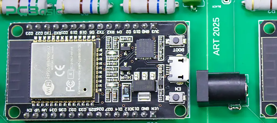
To make PCBs more comprehensible and informative, several signs convey information about certain components and their locations. Here are some of the most used PCB silkscreen symbols:
Component Identifiers: One of the identifiers is to use numbers (1,2,3) or letters (a,b,c) for specific components on the PCB. It eases to locate the circuit assembling.
Polarity Markings: These indicate whether diodes, capacitors or any other components are inserted in the correct polarity, i.e., on the right side up or upside down.
Pin Numbers: To assist in positioning the ICs or the connectors and to confirm that the pins are well arranged, it has numbers alongside the pin of the IC or the connector.
Orientation Markings: Sometimes, technicians use arrows with other kinds of lines or just symbols to point the direction in which the elements of the PCB or the IC have to be positioned.
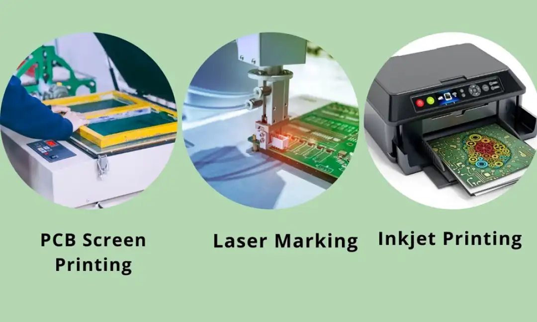
Silkscreen on PCB can be produced by using a screen printing technique that has existed for many years, which entails applying ink through a stencil (or screen) on the surface of the PCB. Imprints of PCB screen printing are highly durable and very accurate. With the increasing complexity of PCB, laser marking and inkjet printing methods are widely used. Laser marking is ideal for fine engravings in logos and other designs, while inkjet markings are mainly for highly accurate designs.
Laser marking is a process that utilizes a laser to burn silkscreen design on the PCB surface without using ink and squeegee. This method is quite precise and suitable for producing delicate details on high-density PCBs. Laser marking is also permanent and can be applied to different material forms.
Another type is inkjet printing, which is more versatile and provides high-resolution silk screening. This is especially applicable for cases where fine, detailed prints and small text are to be printed on complex PCBs. As a result of the features mentioned above, inkjet printing is excellent in areas that require the creation of prototypes quickly.
To ensure the quality of silkscreen on PCB, follow these steps:
Check Component Identification for Accuracy: Make sure all the parts correspond to the label that is present in the design layout.
Check Symbol Positions for Alignment: Check that symbols and text are aligned correctly, whether they fit the component arrangement.
Check Readability and Clarity: In this case, it is important to ensure that the silkscreen used should not be blurred to read or print sections in a manner that could be distorted.
Color Contrast: The contrast between the silkscreen (usually white or yellow) and the solder mask (often green, blue, or black) should be high enough for easy readability.
Use a Magnifying Tool: Utilize a magnifying glass or microscope to inspect small fonts and intricate details in the screen printing.
Compare with Design Files: Compare the PCB screen printing with the design files (Gerber files) to verify that all the labels and markings are as per the design.
At PCBasic, our silkscreen PCB services are tailored for maximum precision. We employ the best PCB screen printing technique to ensure that all the details on your PCB are clear and last for a long time. PCBasic promises accuracy down to each layer of the board, including the top silk screen, bottom silkscreen, and edge silk screen. We can assure you that using our service will make your PCB assembly operation more efficient, non-stop, and of high quality.
Silkscreen PCB is an essential component of electronic circuit PCB. It ensures accurate installation, minimal errors, and high-efficiency production. With the right knowledge about silkscreen on PCB, the types of silkscreens, and the symbols used, you can get quality performance. Fear not. If you are looking for hassle-free silkscreen PCB solutions, try our PCBasic services. We will meet all your manufacturing needs.
 About PCBasic
Time is money in your projects – and PCBasic gets it. PCBasic is a PCB assembly company that delivers fast, flawless results every time. Our comprehensive PCB assembly services include expert engineering support at every step, ensuring top quality in every board. As a leading PCB assembly manufacturer, we provide a one-stop solution that streamlines your supply chain. Partner with our advanced PCB prototype factory for quick turnarounds and superior results you can trust.
Assembly Enquiry
Instant Quote
Phone contact

+86-755-27218592
In addition, we've prepared a Help Center. We recommend checking it before reaching out, as your question and its answer may already be clearly explained there.
Wechat Support

In addition, we've prepared a Help Center. We recommend checking it before reaching out, as your question and its answer may already be clearly explained there.
WhatsApp Support

In addition, we've prepared a Help Center. We recommend checking it before reaching out, as your question and its answer may already be clearly explained there.