Table of Contents
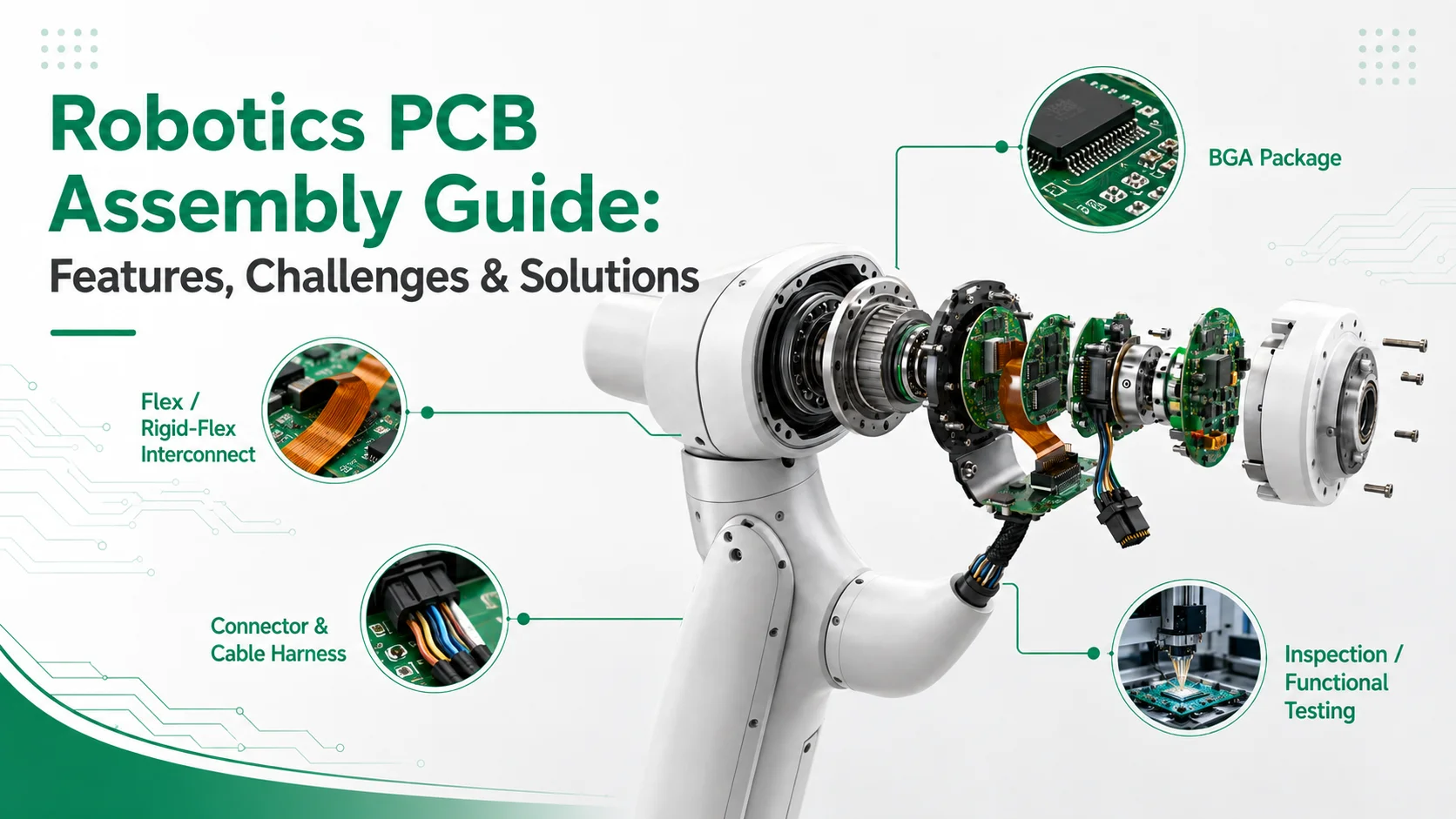
1. What Makes Robotics PCB Assembly Different from Standard PCBA?
2. Which PCB Features Matter Most in a Robot?
3. What Challenges Cause Robotics PCB Assembly Problems?
4. How Do PCBA Manufacturing and Inspection Turn Requirements Into a Reliable Build?
5. Conclusion
6. FAQs
A robot circuit board may look no problem during the single board testing, but after installation, signal problem appears. What makes it changed? Not the board, but its working condition. First, joint movement may continuously stress flexible interconnects and connectors, motor loads increase current and heat generation on the driver board, and the last one, solder joints in BGA packages cannot be fully confirmed through ordinary visual inspection
Therefore, for robotic PCB assembly, just checking whether the component has been correctly mounted and the solder joints are qualified is usually not enough. Suppliers also need to know: where to place each board, which modules are connected, how much load it can withstand, and what’s the conditions requirement of operating and testing of the products. Problems may occur during whole-machine debugging even after the board passes production testing if BOM versions, interfaces, firmware, and testing standards are not verified beforehand.
In PCBasic's robotic PCB assembly services, different boards will undergo assembly, inspection, and testing procedures appropriate to their intended use. This article will introduce the production risks of common boards such as flexible interconnects, BGA packaging, driver and power boards, sensor boards, and other common boards, as well as information customers need to confirm before quoting and production.
What Makes Robotics PCB Assembly Different from Standard PCBA?
Placement quality, soldering and basic electrical checks are still necessary, but these cannot completely reflect the actual working environment of the robot. A joint board is affected by motion and cable force, power board by changing load, and controller need to exchange data with other modules. If we just stop manufacturing evaluation at board-level placement, soldering, and basic electrical checks, we may ignore the actual operating conditions.
Before quoting, a board-role sheet can be quite useful. It keeps track of each board's installation position, attached modules, static or moving condition, electrical load, interface, verification requirements, and pass/fail limit. Using this sheet, we may convert operating conditions into specific manufacturing, inspection, and acceptance points.
A Robot Platform Can Combine Several Board Functions
Different boards in a robot face different risks, so they do not all follow the same manufacturing and inspection plan. The table below can show the main differences.
|
Board type or role
|
Main operating risk
|
Key manufacturing and verification focus
|
|
Vision and controller
|
Dense package, hidden BGA joints and high-speed interfaces
|
Printing and reflow control, X-ray where required, interface testing
|
|
Joint-driver and actuator
|
Current, heat, vibration and connector stress
|
Connector retention, thermal review and defined load testing
|
|
Sensor
|
Signal sensitivity, placement tolerance, calibration requirement
|
Placement control, cleanliness where specified and signal verification
|
|
BMS and power
|
High-current paths, polarity and protection interfaces
|
Polarity checks, solder-joint review and thermal/load verification
|
|
Flex or rigid-flex
|
Bending, unsupported transitions and connector strain
|
Bend control, transition support, strain relief and controlled handling
|
Before making the quotation, the buyer should provide the packaging map, interface and firmware requirements, current or load profile, tolerance of key sensors, battery and protection limits, requirements for flexible board routing and bending, as well as clear qualification criteria based on the project situation.
Movement Changes the Board-Level Risk
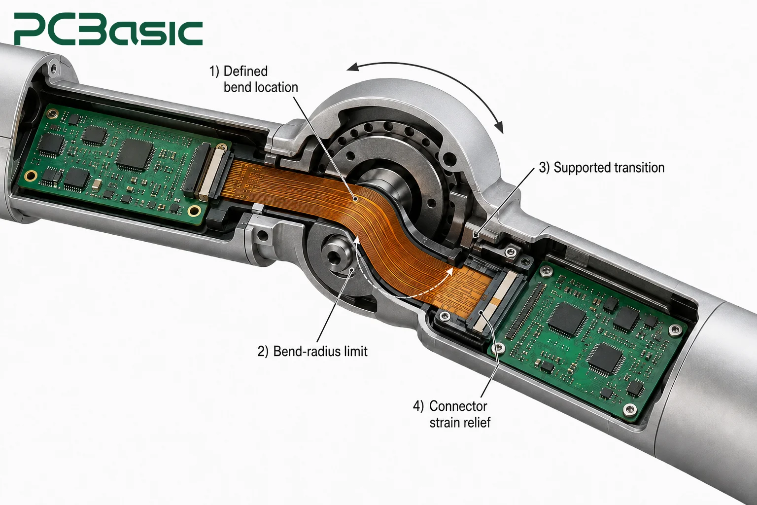
For PCB near the robot joint, we need clarify the bend location and bend-radius limits of the flexible section, and provide support and stress relief for the transition zone and connectors; while stationary controller does not have these requirements. Even if the board can pass the static bench test, repeated movement can expose a weak connector or unsupported flex transition. So buyers should provide the installed routing, motion range, connector orientation, and strain relief before the manufacturing plan is determined.
Mixed Technologies Need Coordinated Planning
A robot often involves multiple assembly contents, including SMT components, BGA packaging, through-hole connectors, flexible or rigid-flexible interconnectors, and the subsequent wiring harness and box build. We need to connect these together by using the same revision and test plan.
Take through-hole connector as example, insertion is merely about placing the components into the holes. Then, the selection of wave, selective, or manual soldering should depend on the type of device, board layout and thermal limitations. We should also consistently state the version of board revision, manufacturing process requirements, test items, soldering method and inspection result in the production records to avoid inconsistent information used in each stage.
Which PCB Features Matter Most in a Robot?
When choosing the PCB structure and packaging form, we need to first consider where this board will be used, what mechanical stresses it will bear, and how it needs to be inspected and tested in the future.
Flex and Rigid-Flex Interconnects Around Moving Joints
When circuits near a robot’s joints need to move along with the structure, standard rigid PCBs are often not flexible enough. In such cases, flexible boards or rigid-flexible boards can be used to connect different modules. During the design phase, it is essential to determine in advance where bending is required and what the bending radius should be, and to provide adequate support and stress relief in the rigid-to-flex transition zones and near connectors to prevent repeated motion from damaging the circuits or connection points.
In drawings and review documentation, we must also specify the actual routing, whether the bending is static or dynamic, the range of motion, and testing requirements. After completing motion testing, verify that electrical continuity, communication, and load conditions are normal. These real settings will also be used by PCBasic to verify the suitability of the flex PCB assembly and testing plans.
BGA Packages on Vision and Controller Boards
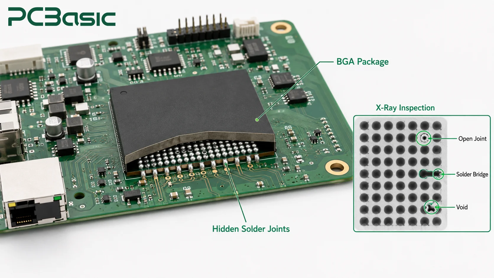
Visual and control boards may use BGA packages to accommodate more connections within a limited space. Because the solder joints are located on the bottom of the package, we cannot fully verify the soldering quality through routine visual inspection. Therefore, a reliable BGA assembly capability requires focused control over solder paste printing, placement accuracy, and reflow soldering curves, and X-Ray inspection should be arranged based on the packaging risks.
You also need to verify whether components are bottom-terminated packages before beginning production, as well as give acceptance criteria and X-ray coverage requirements. For locations with higher risk or more severe failure consequences, we will implement stricter inspection protocols.
Power, Sensor and Communication Boards
These boards do not face the same problems in production. Power boards have to carry current and control heat. Polarity and protection also matter, especially when a battery management system is involved. Sensor boards may need accurate placement or calibration. For communication boards, the main question is whether the interface works and data can pass correctly.
Before production, send the latest BOM and test requirements. A power board needs clear voltage, current, and load conditions. For sensor boards, mark any positions or tolerances that are important. Communication boards usually need a pinout, protocol, firmware, and clear acceptance limits. This information allows the factory to plan the right checks and functional tests.
What Challenges Cause Robotics PCB Assembly Problems?
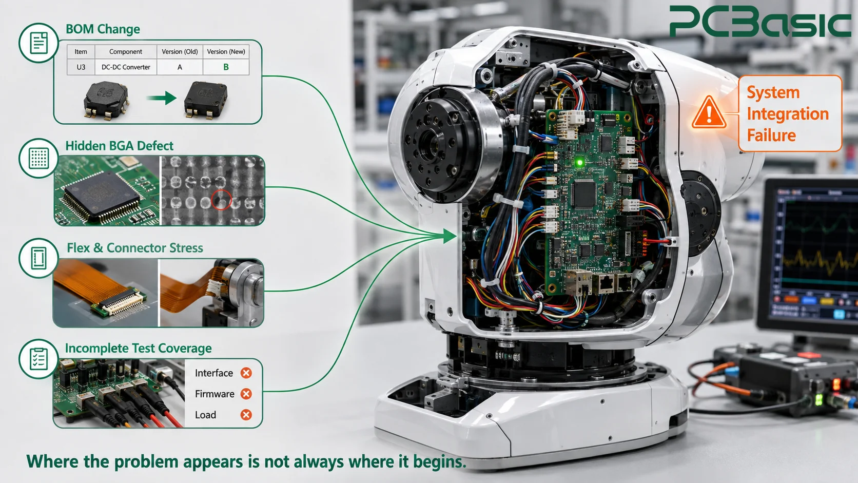
Many PCB issues of robots do not surface immediately after production but are revealed during the final assembly, joint debugging, or actual load operation of the complete machine. Although the problems occur at the end, the causes might have occurred much earlier, such as abnormal BGA hidden solder joints, excessive force applied to the flexible interconnection during installation, failure to record substitute materials synchronously, or lack of testing coverage for the actual interface and load.
Therefore, we cannot merely focus on whether the final test is successful; we also need to trace the possible locations where problems might arise from the aspects of materials, assembly, testing and testing plans.
Hidden Solder Defects Under BGA Packages
The BGA solder joints are hidden at the bottom of the package, and problems such as open circuits, tin bridging and voids are often not visible from the outside. For packages with visible solder joints, AOI can inspect the assembly and welding conditions; however, for BGA and QFN type packages with bottom-end connections, relying solely on AOI is not sufficient. Usually, X-Ray inspection is also required. Which devices to inspect, to what extent, should be determined based on the package type, board card usage and failure consequences.
When determining the detection plan, all bottom-end connection packages and key positions should be sorted out first, and then the coverage range of X-Ray should be clarified. The inspection results should also be corresponding to specific board cards, component numbers and production batches, so as to facilitate traceability when problems occur.
Vibration, Flexing and Connector Stress
Repeated movement may gradually expose some issues that were not obvious in static tests, such as loose connectors, insufficient support in the transition area of the flexible board, or intermittent breaks in the lines during movement. During the test, the board cards, cables, and flexible interconnections can be fixed in the actual installation position, and then allowed to repeatedly move within the specified range. During the process, continuously monitor whether the conduction, communication, and load are stable. After the test, check whether the connector locks and stress release positions are loose or damaged.
Component Sourcing and Revision Changes
After the robot project moves from the prototype stage to trial production and mass production, the original components used may be out of stock, cease production, or need to be replaced. If the replacement materials have not been verified, there may be mismatches in packaging or pins, interference with connectors or casings, changes in electrical performance, impact on firmware, or even loss of the original test standards' significance.
Therefore, the project should use a controlled BOM and a clear approval process for replacement materials, and keep the material records for each production batch. When proposing replacement materials, it is necessary to check the manufacturer's part number, key electrical and mechanical parameters, and firmware compatibility. All changes should be approved before procurement or production release.
Test Coverage That Stops at the Board Edge
Continuity and basic electrical tests can detect issues such as open circuits and short circuits, but they cannot guarantee that the circuit board will function properly once installed in a robot. The controller must be compatible with actual interfaces and firmware; the driver board must operate under specified loads; and sensors and protection outputs must meet the set criteria.
Therefore, functional PCBA testing must be designed with the board’s actual application in mind. You need to provide test specifications, compatible interfaces or fixtures, firmware, operating ranges, and acceptance criteria. PCBasic will configure the corresponding interface, communication, and load tests based on these conditions, rather than applying a single test procedure to all boards.
How Do PCBA Manufacturing and Inspection Turn Requirements Into a Reliable Build?
The final inspection can only confirm whether the finished product passed at that time, but it cannot make up for the absence of recorded substitution material changes, nor can it necessarily detect all deviations left by previous processes. Therefore, quality control cannot be entirely placed on the final inspection. We need to first confirm the materials and versions, control the assembly process, conduct tests at the most likely defect detection points, and finally verify the electrical and functional performance.
The MES system of PCBasic can link the board cards or production batches with material batches, process steps, inspection results and test data. Thus, when there are problems with the overall system integration, engineers can trace back along the records to the specific materials, processes or test results, rather than just seeing a final qualified record.
From BOM and Materials to SMT and Through-Hole Assembly
Once production begins, we first verify that the actual incoming materials match the BOM and version requirements. Surface-mount components are assembled using SMT, while connectors, terminals, and components requiring stronger mechanical fastening are typically mounted using through-hole assembly.
The soldering method is selected based on the component type, board layout, production volume, and heat resistance requirements. Common methods include wave soldering, selective soldering, hand soldering, and through-hole reflow soldering. Throughout the process, production records should document the board version, BOM, material batch, soldering method, and inspection results to prevent inconsistencies in the information used across different production steps.
SPI, AOI, X-Ray and First-Article Inspection
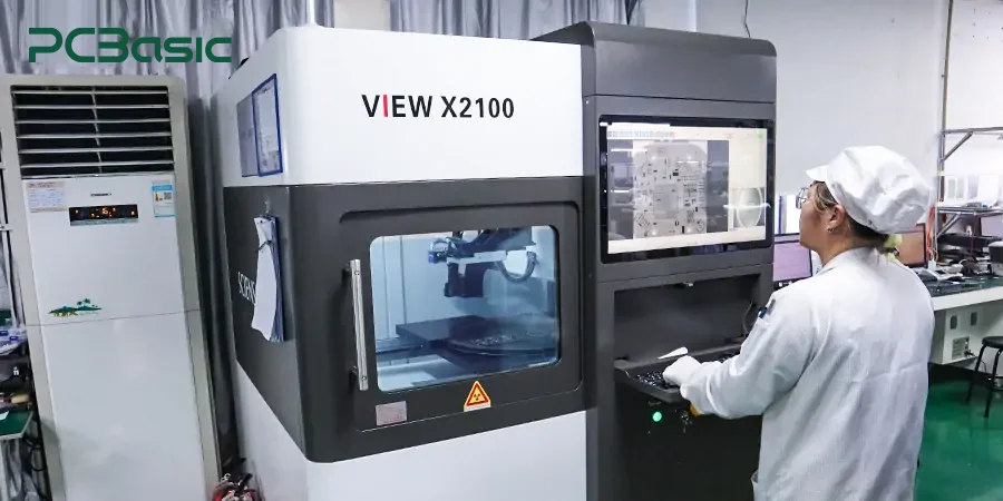
Before mounting the components, SPI will check the volume, position and shape of the solder paste to prevent any obvious abnormalities from entering the reflow soldering process. After the assembly is completed, AOI is used to check the visible positions of the components and solder joints, while X-Ray is used to examine the hidden solder joints beneath BGA and other packages. Before officially expanding production, we will also conduct first-piece inspections to confirm the assembly results and related production data.
The problems solved by different detection equipment are not the same, so it is necessary to arrange them according to the actual risks. The project plan should clearly specify which packages and defects are to be inspected by SPI, AOI or X-Ray. The accompanying solder joint analysis videos can help you understand the specific detection process.
Functional Testing and Digital Traceability
Functional testing can verify interface communication, signal response, load output or protection logic according to the defined test plan. MES and inspection records preserve the context, allowing a fault to be traced to a board, component reference or material lot, process step and test result.
Final Assembly, Box Build and Cable Harness Integration
For some projects, in addition to PCBA, the following tasks need to be completed: wiring harness processing, module connection, and shell assembly. During the assembly process, it is necessary to confirm that the wiring sequence, connector orientation, and installation position are correct, and also to check for shell interference and fastening conditions. After completion, functional tests should be conducted as required.
When making the quotation, you need to provide the drawings of the enclosure and cables, the definition of connectors, the tightening requirements, and the testing requirements after assembly.
Conclusion
Reliable robot PCB assembly is not only about correctly soldering components onto the circuit board, but also involves arranging the assembly, inspection and testing based on the purpose and actual working conditions of the board. For moving parts, attention should be paid to the bending radius of flexible interconnections, structural support and stress release; for BGA and other bottom-end connection packages, the welding process needs to be controlled and hidden solder joints should be inspected; for power, sensing, control and communication boards, the actual interfaces and load verification functions should be combined.
Before the quotation and manufacturing review, the customer should provide the latest Gerber files, BOM, CPL, assembly drawings and version records, and explain the requirements for bending, testing, interfaces, load, enclosure and cables, etc. At the same time, they should confirm the quantity and delivery date. Through the PCBasic engineering review, these materials can be uniformly checked before production, thereby enabling early confirmation of assembly, testing, inspection and overall integration plans, and reducing the risk of rework and joint debugging issues when the project transitions from prototype to mass production.
FAQs
Q1: What should a robotics PCB assembly package include?
A1: Include Gerber, BOM, pick-and-place/CPL, assembly drawings, package map, bend requirements, tests, interfaces, loads, enclosure or cable details, revision, quantity and schedule.
Q2: How should flex interconnects around robot joints be reviewed?
A2: Review routing, static or dynamic bend designation, bend limit, transition support, strain relief and motion range. Define a movement check that monitors the relevant signal.
Q3: Why Is X-Ray Commonly Used for BGA PCB Assembly?
A3: BGA boards generally require a defined hidden-joint inspection strategy, with X-ray coverage determined by package and product risk.