Global high-mix volume high-speed PCBA manufacturer
9:00 -18:00, Mon. - Fri. (GMT+8)
9:00 -12:00, Sat. (GMT+8)
(Except Chinese public holidays)
Global high-mix volume high-speed PCBA manufacturer
9:00 -18:00, Mon. - Fri. (GMT+8)
9:00 -12:00, Sat. (GMT+8)
(Except Chinese public holidays)
HomePage > Blog > Knowledge Base > What are PCB Test Coupons?
In the world of electronic manufacturing, the performance and quality of a circuit board is particularly important. One such tool for testing circuit boards is the PCB test coupon, which is efficient and low cost.
Keep reading and learn more about what a PCB test coupon is, its location and features.

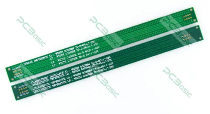
A PCB test coupon is a representative sample or area specially used for testing and verifying the production quality. It is also known as a quality conformance coupon or QC coupon. The test coupon can verify a number of performance indicators of the circuit board and test specific parameters during the production process, ensuring that the circuit board meets the standards of high performance and high reliability.
In PCB manufacturing, the test coupon simulates the structure and number of layers of the main PCB, but it is separate from the functional area. It will not affect the function of the main board when conducting electrical, mechanical and environmental tests, which can greatly ensure the quality of the board and its long-term use.
PCB test coupons are usually located on the edge of the PCB panel or are produced with the main board as a separate unit.
As mentioned above, they are only used to test and verify the manufacturing and electrical performance, having no other circuit functions. Therefore, in order to save space and reduce the volume of the equipment, the PCB test coupons will be cut off and performed test independently after production without affecting the normal function of the main board. These test coupons are placed on the edge of the PCB for easy cutting and testing without affecting the main circuit. Some manufacturers also choose to make test templates on adjacent separate boards, especially if repeated testing is required or more complex test Settings are required.
The location of the PCB test coupon is designed not only for the protection of the main board, but also for the convenience of production. In the design of multi-board panel layouts, the test coupons are usually located at the shared edges of the panel. By testing one coupon, we can know the overall quality of multiple boards, which saves materials and time.

PCB test coupons can be used for a variety of circuit tests to ensure the electrical and mechanical integrity of the board. It is a key method to verify the quality and structure of the board, including the following primary tests:
Electrical Testing: PCB test coupons can test circuit board's continuity, resistance, and insulation properties to detect the copper trace faults or connection problems.
Thermal Stress Testing: The test coupon is subjected to extreme temperature variations to assess durability and detect potential delamination or warping issues.
Solder Joint Testing:The strength of the solder joint of the test coupon is tested, detecting its soldering strength and bonding quality.
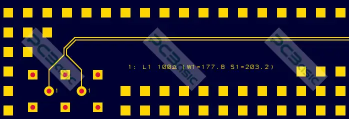
Impedance Testing: For high-speed circuits, impedance control is essential. PCB test coupons can help measure impedance levels, ensuring they are within specified tolerances to maintain signal integrity.
Mechanical Testing: Test coupons also undergo mechanical stress testing to simulate conditions the PCB may encounter during assembly or use, such as bending or flexing. This testing helps ensure structural integrity.
Thickness and Plating Checks: PCB test coupons allow manufacturers to measure copper plating thickness and confirm that each layer’s thickness meets specifications. Thickness testing is also commonly performed on weld test plates in metalwork to verify structural soundness.
The design of PCB test coupons can accurately reflect the structure of the main PCB. Its design includes multi-layer structure, through holes and copper traces, etc., which can most truly simulate the performance of the main PCB.
In multilayer PCBs, the test coupon typically includes a structure that matches the configuration of each layer to test the alignment and thickness. For high-frequency or high-speed PCBs, the test coupon is designed with a copper trace with controlled impedance to ensure signal integrity.
Size is also crucial in the pattern design, and it must closely match the number of layers of the board and the layout of the lines to ensure the accuracy of the test. Test coupon structures typically include holes, wiring, and pads for electrical and thermal performance testing. These structures ensure that possible defects, such as bad solder joints or delamination problems, are detected at the final production stage.

PCB test coupons play a great role in evaluating and ensuring PCB manufacturing quality, bringing many advantages to the production of circuit boards.
PCB coupons can not only detect the key parameters of the circuit board, but also simulate the actual work situation to help predict the boards’ working performance, finding potential problems in advance during the production process to modify it in time to ensure that the final production of the circuit board meets the industry and customer standards.
In addition, PCB test coupons are small and representative. Using them to detect not only can not affect the function of the main board, but only test part of the circuit instead of testing the entire, which greatly reduces the production cost.
But there are some limitations to PCB test coupons. Because it only performs partial tests on specific areas of the PCB, the test results do not represent the quality of the entire board. Moreover, because PCB test coupons are produced at the same time as PCBs, their design and integration require additional effort and increase the complexity of the board layout.
PCB test coupons are an integral part of electronics manufacturing, especially in industries with stringent requirements for reliability and safety. These dedicated test areas simulate the structure of the main PCB, allowing manufacturers to conduct comprehensive testing without compromising the integrity of the main board. By detecting potential defects early in the production process, PCB test coupons help improve quality, reduce failure rates, and ensure that the final product meets stringent regulatory standards.

Assembly Enquiry
Instant Quote
Phone contact

+86-755-27218592
In addition, we've prepared a Help Center. We recommend checking it before reaching out, as your question and its answer may already be clearly explained there.
Wechat Support

In addition, we've prepared a Help Center. We recommend checking it before reaching out, as your question and its answer may already be clearly explained there.
WhatsApp Support

In addition, we've prepared a Help Center. We recommend checking it before reaching out, as your question and its answer may already be clearly explained there.