Global high-mix volume high-speed PCBA manufacturer
9:00 -18:00, Mon. - Fri. (GMT+8)
9:00 -12:00, Sat. (GMT+8)
(Except Chinese public holidays)
Global high-mix volume high-speed PCBA manufacturer
9:00 -18:00, Mon. - Fri. (GMT+8)
9:00 -12:00, Sat. (GMT+8)
(Except Chinese public holidays)
HomePage > Blog > Knowledge Base > Efficient PCB Reverse Engineering Services | PCBasic
One innovation, debugging, and legacy system support is PCB reverse engineering. Reverse engineering a PCB means a type of analysis made to replicate the design or the functions of a given circuit to enhance the arrangement of a pcb’s structure. From analysis, companies come up with ideas for circuit layouts, components of configurations, and electrical pathways, thus opening chances for maintenance or alteration without original design files.
With advanced PCB reverse engineering tools, engineers can efficiently trace electrical connections and components, generate schematics, and reconstruct a complete PCB layout. It is a highly valuable approach for innovative industries that must be compatible with legacy systems in terms of optimization, cost savings, and protection of intellectual property.
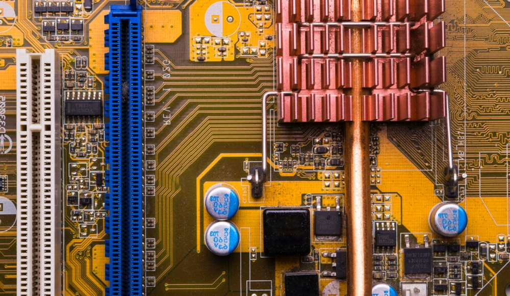
PCB reverse engineering is a process that considers a study of a target PCB, reverse analysis, and the production of technology during the creation of a PCB. Such a technology is applied to the identification as well as attainment of the structural and functional design of certain products. The technology of PCB reverse engineering could further be used to identify the process in which a product will pass. All this information would help a firm develop similar products with equal capabilities and functionalities through pcb reverse engineering services. In reverse-engineered PCBs, the firms would be sure that they would not replicate the product. Much more critical to the process is PCB reverse engineering, which is when any company cannot find a way to get the detailed designs of a particular product.
The most common method used by a company when reverse engineering a PCB is disassembly. From the disassembly, a company will be in a position to come up with documentation regarding the sample PCB used by different teams for various processes and reviews. The documentation shall contain all information regarding the design of the product and how it operates.
This would benefit them in making similar PCBs that function better than those of their competitors. They can, besides satisfying the customers of competitors even better, also improve their own PCBs' functionality. They can identify and improve upon obsoleted parts, security issues, and bad design through the reverse engineering circuit boards.
Let's take a closer look at the advantages of PCB reverse engineering.
· Save the required PCBs: You would find, in many cases, an old or obsolete PCB that supplies power to some portion of the machinery or equipment. Now, if this is your only PCB that supplies the power, then getting it replaced can become quite cumbersome, especially when it needs repair. PCB reverse engineering may help you save the required PCBs in the system and replicate it for further use if needed.
· Collect detailed information on PCBs: Currently, CAD information and documentation for all designs of PCBs are mandatorily enforced. That makes them easily reviewable and understandable by other people as well. Sometimes, though, PCBs carry no information available to them. PCB reverse engineering is what can help you understand the circuit board diagram schematic and design information available on the PCB. That will enable you to do your personal documentation, through which you can repair it and also reproduce it.
· Reduced dependence on professional experts: If something went wrong in your PCB, you would normally look to a professional for some kind of help. They will fix and correct them. This would be uncomfortable for you since others, not professionals, could fix the problems found in your PCB. You will receive important information related to your PCB through PCB reverse engineering service, and you will come across components that will pose a problem without an expert doing so.
· Find loopholes in a competitor's designs: You are always finding ways of making your product more efficient and better than what your competitors are offering as you design PCBs. By reverse engineering a competitor's PCB, you can spot their loopholes and make yours much better. You can still build more efficient PCBs even for other purposes that aren't selling.
· Create PCBs with a competitive cost: In case you have an opponent that sells you at a higher price, you could reverse engineer the PCB so you find out about its cost to produce such a product that closely could be produced. Having this in mind would aid you in making related PCBs that will charge a relatively low cost, hence attracting many more customers and opening big markets for yourselves.
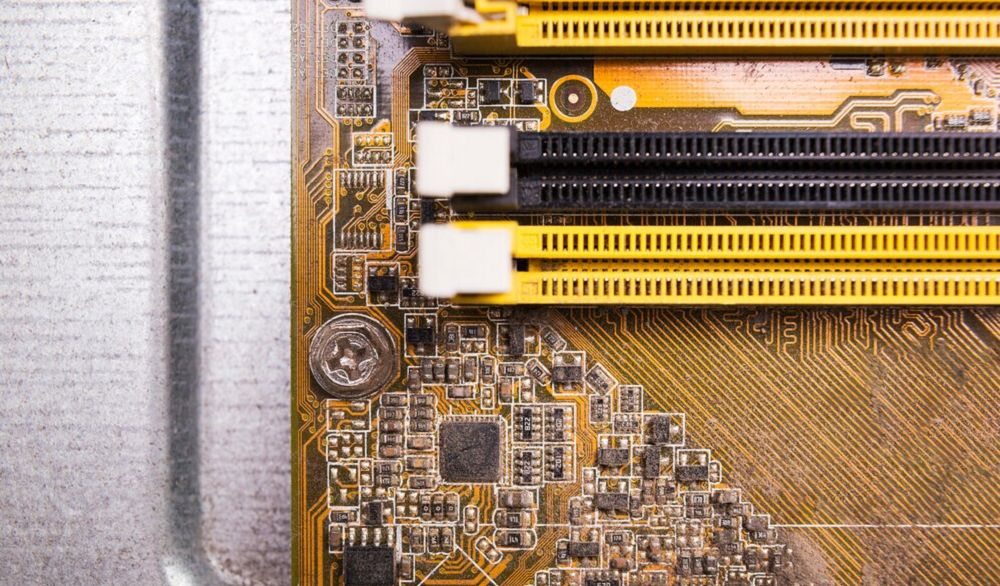
To read this article, you must be interested in PCB reverse engineering. PCB reverse engineering services are widely used in modern electronics manufacturing. This is especially important in situations where original design documentation is lacking, or where companies need to adapt or innovate quickly. Here are some scenarios where PCB reverse engineering may be used:
There are old electronic products with no original documentation, and although they are old, many of these products are still in use today. When they need to be repaired, or when a manufacturer wants to reproduce these series of products, PCB reverse engineer technology is needed at this time. With the technique of circuit board reverse engineering, these systems can be recovered and re-manufactured to produce updated design formats.
PCB reverse engineer can also be used to do competitive product analysis. Many companies often use PCB reverse engineering to study the circuit design of competitors, which is of great value for product comparative analysis, technological innovation or identification of cost optimization programs.
Reverse engineering circuit boards can also be used for low-cost redesign and optimization. By reverse engineering PCBs, companies can optimize existing designs, improve performance or choose more cost-effective components. This method is especially suitable for design improvement before mass production. So how to do PCB reverse engineering?
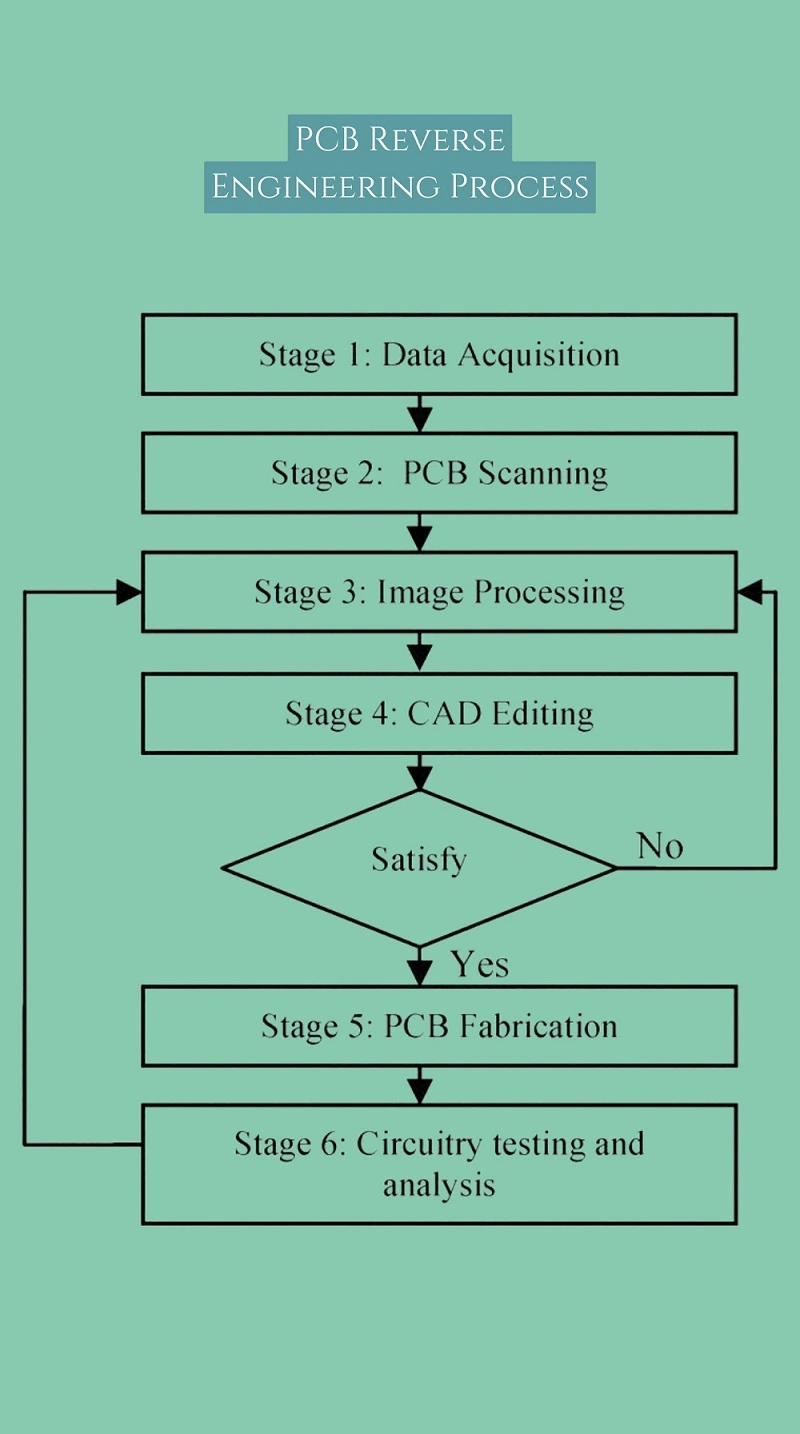
Now, let us discuss this process of reverse engineering a PCB in detail.
1. Preparations
In the process of reverse engineering a PCB, you have to draw, scan, and photograph the PCB board. When you take pictures, you can make sure you get both sides of the board. This, too, is very crucial to catch it with a black background as any kind of light background, such as white, appears to be copper. Given that the PCBs are produced in holes, take care that the background not be visible in the holes.
2. Photograph PCBs
You will use good cameras to capture even the smallest details of your PCB; a smartphone camera or even a digital camera will do. It then involves photography and scanning the images, meaning you may have to be detailed when color-switching or otherwise image editing those images at times. You will do this most of the time when complicated layouts are involved. An easy PCB layout can be sketched on a piece of paper. Graph paper is used for this purpose. During the drawing of the PCB, the actual scale must be captured.
3. Part-Wise Analysis
Let's first have a well-prepared PCB board before entering this process of reverse engineering that would cover orchestration as well as strategic manipulation of many tools that may be called upon so as to condition the PCB to itself in detail.
· Cleaning the PCB is excellent once the photographs have been taken. Removing dirt/dust/particulate matter that could potentially destroy sensitive details in other inspection stages is indispensable.
· Protective and conformal coatings should be removed step-by-step only where necessary and justified to expose underlying components bare to show the intricate traces to be examined.
· Desoldering and removal of components is very delicate. It should, therefore, be done with caution since it enables the traces and connections to be observed in depth.
4. Create a Bill of Materials (BOM)
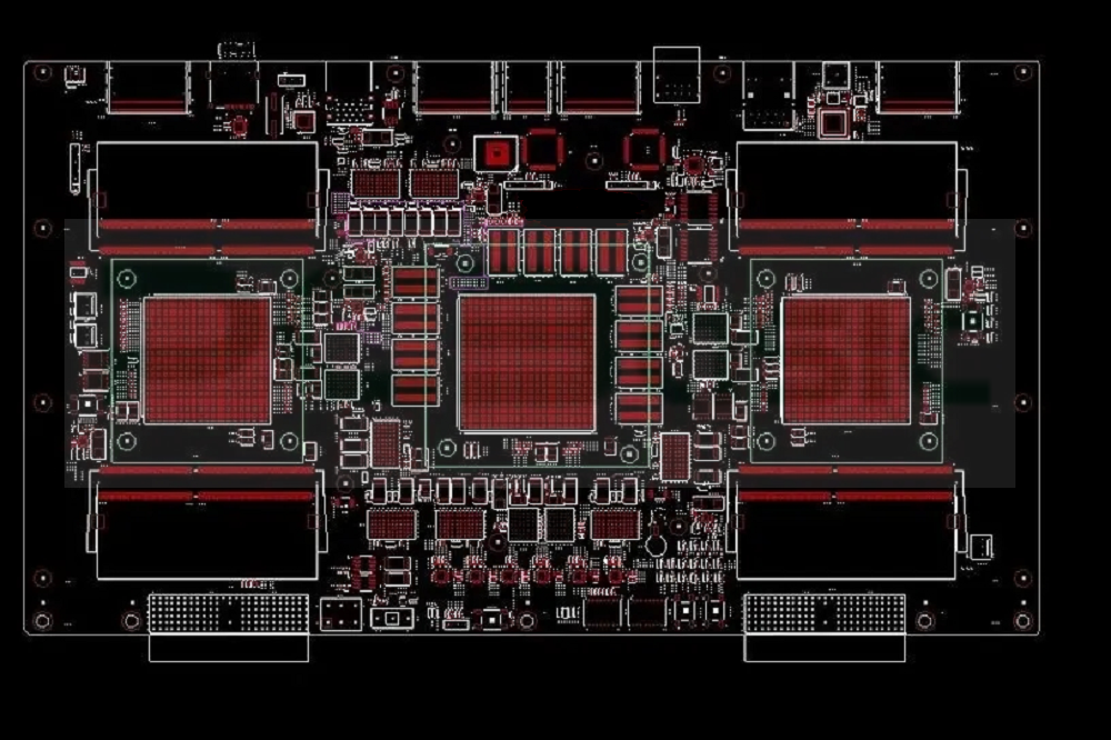
A BOM is a comprehensive, itemized list of each part used in the PCB's design and manufacturing that contains information such as specifications, quantities, and reference designators. One should be extremely careful and precise while working with a BOM because it determines whether appropriate parts have been used and properly assembled when creating the board. It also involves component listing and obsolescence management. In such a matter, BOM proves helpful. Tasks in curating a BOM along the way of PCB reverse engineering:
· Identify all the parts: A very long sequential process of all and every component of PCB must be undergone by engineers. In this process, every component would be accurately dissected based on what function it performs.
· Reference designator assignment: Every component on the PCB must be assigned a unique reference designator. These are names that then propagate through the circuit board schematic of the PCB, layout, and BOM.
· Source for parts: In addition to part-specific information, a BOM should contain the manufacturer's part number and appropriate screened approved vendor list.
5. Schematic generation
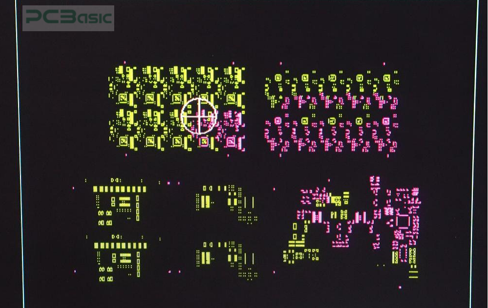
A PCB schematic for the circuit board is developed through the following procedure:
· Tracing and understanding connections is a very careful task. It involves tracing connections between various components that are on the PCBs. If the PCB is multilayered, then this task becomes very, very tiresome. Understanding the connections can also be done through optical inspection tools that are equipped with high precision and magnification.
· Visual inspection of the PCB component to a high-resolution level. The task construed it as the physical feature and inherent property, which is value, type, and use.
· A digital model needs to be created that would represent the tapestry of the PCB. Ideally, different PCB reverse engineering software can interpret physical components into a digital model.
6. Rebuilding PCB Layout
PCB configuration reconstruction includes the following:
·Install all the components on the PCB very carefully, considering the proper arrangement, with precise planning and design. Along with that, integration with both through-hole and surface-mount devices should be treated properly.
·The electrical routings and connections have to be done very accurately, and the schematic has to provide guidance to achieve this for proper connections.
·Verification of design is the last stage of reconstruction. The engineers verify the design correctly. It includes various activities like checking the electric processes, performance of design, etc.
7. Documentation
The entire process of reverse engineering the PCB needs to be properly documented. Every appropriate curating and maintenance that follows during the whole process would have the utmost significance. Absolute precision and consistency would be warranted in the final design of the PCB. Everything observed in the whole process has to be noted. X-ray checking would let the engineers check behind the PCB in terms of how its inside framework was actually structured.
It, therefore, results in the generation of a higher accuracy level and of high quality in reverse engineering. The process involves the creation of files in the forms of images, bitmaps, and Gerber files. After reverse engineering, the files are synthesized in such a way that they become viewable for functionality testing, and then the validation of the design follows.
PCB reverse engineering employs a range of manual tools and methods, including:
·Signal processing techniques: Spectral analysis and Fourier transforms can be utilized to determine various frequency domain features of source noise that impact signal integrity.
·Noise margin analysis: Noise margins can also be done. It can ensure that digital noise signals are at the required levels. It will minimize the possibility of data corruption.
There exists:
· Professional electronic design automation tools are able to provide smooth schematic generation, BOM generation, and layout reconstruction.
· The high-resolution microscopes, cameras, etc., along with the zoom facility for optical inspection of the PCB, are optical inspection tools.
· X-ray Inspection Equipment facilities an inner layer, which could reveal the inner work of the PCB board.
When reverse-engineering a PCB, a variety of software tools are used to help engineers digitise, analyze and reconstruct the board efficiently and accurately. The following are common software tools used in the PCB reverse engineering process:
PCB design kits, such as Altium Designer, KiCad and OrCAD, are industry standard schematics and PCB layout reconstruction tools.
Gerber file editor: Tools such as ViewMate, GC-Prevue, and GerbView for editing or regenerating Gerber files.
Dedicated reverse engineering software such as RECap, InspectAR, and PCBLib assist in identifying component connections, generating netlists, and mapping circuit logic.
Signal tracing and circuit simulation tools: For high-speed or complex circuit designs, engineers use simulation software such as LTspice or Advanced Design System (ADS) to verify and optimize signal behavior after completing PCB reverse engineering.
These PCB reverse engineering tools help reduce errors, increase efficiency, and ensure high accuracy when replicating the original design.
PCB reverse engineering has excellent means for quality enhancement in the product, so it solves all the problems that may have arisen at the hardware end or simply be compatible with the present system. The process will bring precision in engineering and technology at the time of presenting these replicas or improved versions of the existing designs. The PCB reverse engineering service is part of the toolbox for survival in dynamic landscapes in tech and transforms hardware into optimized solutions.

Assembly Enquiry
Instant Quote
Phone contact

+86-755-27218592
In addition, we've prepared a Help Center. We recommend checking it before reaching out, as your question and its answer may already be clearly explained there.
Wechat Support

In addition, we've prepared a Help Center. We recommend checking it before reaching out, as your question and its answer may already be clearly explained there.
WhatsApp Support

In addition, we've prepared a Help Center. We recommend checking it before reaching out, as your question and its answer may already be clearly explained there.