Global high-mix volume high-speed PCBA manufacturer
9:00 -18:00, Mon. - Fri. (GMT+8)
9:00 -12:00, Sat. (GMT+8)
(Except Chinese public holidays)
Global high-mix volume high-speed PCBA manufacturer
9:00 -18:00, Mon. - Fri. (GMT+8)
9:00 -12:00, Sat. (GMT+8)
(Except Chinese public holidays)
HomePage > Blog > Knowledge Base > The Ultimate Guide to PCB Antenna| Design, Types, and Applications
Antennas play an important role in connecting devices without any cables. One popular type of antenna is the circuit board antenna, which uses the conductive traces on a PCB as a conductor. The PCB antennas are super convenient and they are used on various electronic devices such as smartphones and IoT devices.
Circuit board antennas are becoming more important as modern electronic devices require more compact and cost-effective designs. Their small size and low cost make them attractive for manufacturers who want to optimize space without sacrificing performance. These antennas also simplify the design process by eliminating the need for external antennas.
Let's explore circuit board antenna types and their applications. We will also learn their benefits and limitations and compare chip antennas vs PCB antennas.
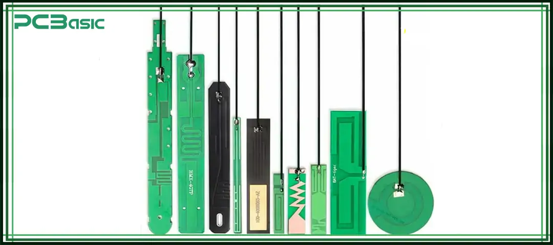
There are many different types of PCB antennas available in the market. Each of the antenna offers unique features and applications. It is important to know PCB antenna types so you can choose the right one for your needs.

Here are common circuit board antenna types:
A Monopole antenna is one of the simplest types of PCB antennas. They consist of a single radiating element that is mounted vertically above the ground plane of the PCB. It is small in size around half the length of the wavelength. A monopole antenna is omnidirectional, which means it can radiate in all directions.
· The design is straightforward and easy to manufacture.
· Monopole antennas work on a uniform radiation pattern that makes them reliable choices for many applications.
· Performs well in a wide range of frequencies
Monopole antennas are used in various devices such as mobile phones, wireless communication devices, and RFID systems. Their simple design makes them ideal for applications that have limited space.
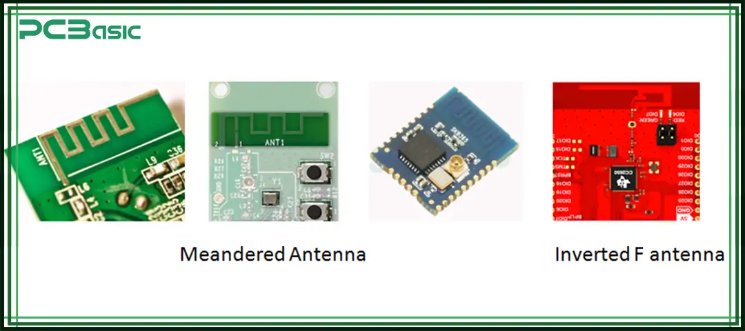
The Inverted-F Antenna is a variation of the monopole antenna. It features a short radiating element that is bent back towards the ground plane. This forms an inverted "F" shape and this is where it got its name from. IFA is even smaller than a Monopole antenna, which makes it suitable for small devices and applications.
· The IFA takes up less space than traditional monopole antennas.
· It has better impedance matching, and it can operate on lower frequencies.
· It can be easily integrated into various PCB layouts.
IFAs are widely used in mobile devices and Wi-Fi applications. They are super small which makes them suitable for modern electronics that need wireless communication.
A meandered antenna has a zigzag or meandered shape. This unique design helps them achieve specific radiation patterns and bandwidths even with a small footprint on the PCB.
· The unique zigzag design makes a longer antenna in a smaller area.
· These antennas can cover a broad range of frequencies.
· They can be easily printed on PCBs at less cost.
Meandered antennas are used in IoT applications and RFID systems. They are ideal for devices communicating on different bands, as they can operate on many frequencies.

A dipole antenna is made of two conductive elements of the same length. They are joined in a straight line with a gap. Its elements are created on PCB with metal traces. Dipoles work as reference antenna for measurements most of the time.
· Dipole antennas emit signals in two directions, which makes them ideal for many applications.
· Their manufacturing process is simple.
· Dipoles offer a decent gain of around 2.15 dBi.
Dipole antennas are simple and suitable for various frequencies. This makes them the first choice for many applications, such as television broadcasting and Wi-Fi networks.
A patch antenna is also famous as a microstrip antenna. It is a flat rectangular antenna with a metallic patch on one side of the PCB and a ground plane on the other. The size and shape of the patch determine its operating frequency. Patch antenna is commonly used for directional communication.
· Patch antennas are thin and lightweight, making them ideal for small devices.
· They can be easily printed on PCBs.
· Patch antennas offer high gain and can be designed for specific polarization.
Patch antennas are suitable for GPS devices and satellite communications. They are ideal for applications that need precise signal transmission, as they can easily operate on specific frequencies.
A loop antenna is like the loop of a conductive material. It can be circular or rectangular in shape. The loops can be printed on the PCB but are sensitive to magnetic fields. A loop antenna can operate at various frequencies and it is ideal for low-frequency applications.
· Loop antennas can be very small in shape without any impact on performance.
· They emit signals in all directions.
· Loop antennas can cover various frequencies.
Loop antennas are commonly used in RFID systems, NFC applications, and various wireless communication devices. They are super versatile and small, which makes them a reliable option for modern electronic applications.
A slot antenna is created by cutting a slot in the ground plane of a PCB. Then this slot radiates electromagnetic waves. Also, the dimensions and shape of the slot can tell a lot about the characteristics of the antenna.
· Slot antennas are made on the ground plane of PCB, saving space
· They offer good bandwidth and radiation patterns.
· Their design can be customized to fit in the existing PCB layouts without a complete redesign.
Slot antennas and wireless communication systems go hand in hand. These include automatic radar systems and Wi-Fi devices. These antennas can operate efficiently even in small spaces, which makes them suitable for compact devices.
PCB Antenna is an important element for modern electronic and compact devices. They perfectly align with cost-sensitive, durable, high-performing, and convenient transmission systems. With its outclass efficiency and super flexibility, it offers a range of stand-out features, making it an effortless signal conduction element.
Here are some of the key benefits of using PCB Antennas:
PCB Antennas saves costs by cutting down the need for several external components. It doesn't require a separate connectivity element to get integrated into circuits. This further simplifies the production, eliminating the extra effort of adding external components. These are built during the PCB manufacturing process to save additional costs on the assembly and incorporation.
The most striking feature of PCB Antennas is their small, tiny, and exclusive sizes. They require minimal to low space volumes as they're etched directly into the circuits. The devices with compact, confined, and limited spaces are ideal for PCB Antennas. IoT, wearables, smart devices, and GPS are some of the best uses acquired due to their sizes.
PCB antennas can be customized for a range of devices and operations. This customization includes sizes, shapes, trace patterns, and frequencies according to the device. Engineers can also fine-tune their frequency to support multiple or a set of frequency bands to operate in wireless communication and other systems, including Wi-Fi & GPS.
Given its customization, they support a scalable and highly consistent set of wireless systems. Once the PCB antenna design is completed, it can be replicated into various units (thousands or hundreds) without external production.
As the PCB Antenna structure supports the direct integration onto the circuit board, it further provides a consistent and high-performance output across all the units. It only requires additional components to maintain its consistent operations throughout the process.
There are more than five types of antennas, and loop antennas are the perfect components to provide flexible antennas. They can easily survive bending and stretching without breaking into tiny parts when stressed or pulled.
The direct integration into the circuit is the primary factor in driving sustainable and less susceptible mechanical damage characteristics. They have no external connections, contain no moving parts, and are helpful for rugged environments.
PCB antennas operate at a high direction-oriented module as it has no distributive and tangled pathways due to direct integrations. This reduces the signal path losses effectively and directs the traces in a more efficient transmission. PCB Antennas have been the best performers for high-frequency devices with no external connection circuit architecture.

PCB antennas also have some limitations along with their benefits. Below are some limitations of PCB antennas that you should also consider during the designing process:
PCB antennas work in a shorter range than external antennas. So, they are not ideal for applications that need long-distance communication.
The performance of a PCB antenna depends on its design, such as the size of the PCB and the antenna layout. If the design of the antenna is not reliable, it can affect signal strength and create interference.
PCB antennas work better on different frequency bands. But if your antenna supports multiple frequencies, it can complicate the process. It can also affect the performance.
PCB antennas can not handle high power like other large or external antennas. This means that you cannot use them for high-power transmission applications.
Many PCB antennas can be less directional. This means they radiate signals in all directions. This can reduce their efficiency in applications that need focused signal transmission.
It can be challenging to tune a PCB antenna so they perform well. Also, you must retune every time you change the board size or layout. This can lead to more time and effort in the design process.
 About PCBasic
Time is money in your projects – and PCBasic gets it. PCBasic is a PCB assembly company that delivers fast, flawless results every time. Our comprehensive PCB assembly services include expert engineering support at every step, ensuring top quality in every board. As a leading PCB assembly manufacturer, we provide a one-stop solution that streamlines your supply chain. Partner with our advanced PCB prototype factory for quick turnarounds and superior results you can trust.
If you want your PCB antenna to work well, you will have to make sure that you go for a reliable design that meets your specific needs. Here are some things to consider before designing your PCB antenna:
· Frequency band: Antennas work on frequency bands suitable for different communication ranges. So when designing your antenna, it is important to design it to work with a suitable frequency range, such as 2.4 GHz for Wi-Fi or Bluetooth. When you go for the correct frequency band for your PCB antenna design, you can enjoy better signal strength and transmission quality.
· Ground plane: The ground plane is also an important PCB antenna design. The plane can affect the antenna's performance by disturbing the radiation pattern and impedance. Make sure to consider a good design for a ground plane for better signal transmission and less interference.
· Impedance matching: Impedance matching can make sure that the antenna works well with connected circuits. Poor impedance matching can result in signal loss or less efficiency. Designers should carefully match the antenna's impedance with the transmission line. This is usually around 50 ohms for good performance.
· PCB antenna simulation and prototyping: Before you finalize the design, it is important to use simulation tools to test antenna performance. These tools test the behavior of the antenna on different parameters. These include radiation patterns and impedance. After simulation, prototyping also tests the antenna in real-world scenarios to make sure the design meets the standards.
· Environmental factors: Environmental factors can also affect the performance of PCB antennas. Different surrounding items can affect the signal strength of antennas. These include metal objects or the enclosure of the device. Make sure to consider this when placing the antenna on the PCB and in the device housing.
Modern electronics for wireless communication can work on both chip and PCB antennas. However, they can have different features and purposes. Let us explore more about chip antenna vs PCB antenna.
· Chip antenna: A Chip antenna is a pre-manufactured small antenna module. It is simple to place this antenna on the PCB like any other electronic component.
· PCB antenna: A PCB antenna is directly printed or traced onto the surface of the PCB itself during the board's design process.
Let's look at the detailed comparison of Chip antenna vs PCB antenna:
Feature Chip Antenna PCB Antenna
Size and Form Factor: Very small and lightweight, ideal for compact devices. It varies in size; it is generally larger, but you can redesign it to fit specific layouts.
Performance: Often pre-tuned for reliable performance but may have limitations due to size. East to customize for specific performance characteristics like gain and bandwidth.
Ease of Integration: Easy to integrate with mounting pads for direct soldering onto PCBs. Requires careful design and layout considerations for optimal placement.
Customization Limited customization options Highly customizable based on PCB design needs
Applications: Mobile phones, Bluetooth devices, IoT devices, Wi-Fi modules, wireless sensors, RFID, drones, consumer electronics
PCB Antennas made from printed circuit boards are very important in wireless communication. PCB antenna designs range from super compact to running applications and are cost-effective. They can be anything from a simple monopole design to the more complex patch and slot antennas. They give flexibility in design but have reliable performance.
Understanding various PCB antenna types will enable you to make more sense when it's time to select just the suitable antenna that will suit your application. As technology advances, we can only expect to see even more innovative and sophisticated PCB antenna designs

Assembly Enquiry
Instant Quote
Phone contact

+86-755-27218592
In addition, we've prepared a Help Center. We recommend checking it before reaching out, as your question and its answer may already be clearly explained there.
Wechat Support

In addition, we've prepared a Help Center. We recommend checking it before reaching out, as your question and its answer may already be clearly explained there.
WhatsApp Support

In addition, we've prepared a Help Center. We recommend checking it before reaching out, as your question and its answer may already be clearly explained there.