Table
of Contents
1. How a Wireless Charger Transmitter Board Works
2. Key Components of a Wireless Charger PCBA
3. Matching the Board and Coil to the Charging
Pad
4. Assembling the Board, Coil, and Enclosure
5. Testing Charging Power and Temperature
After Assembly
6. Conclusion
7. FAQs
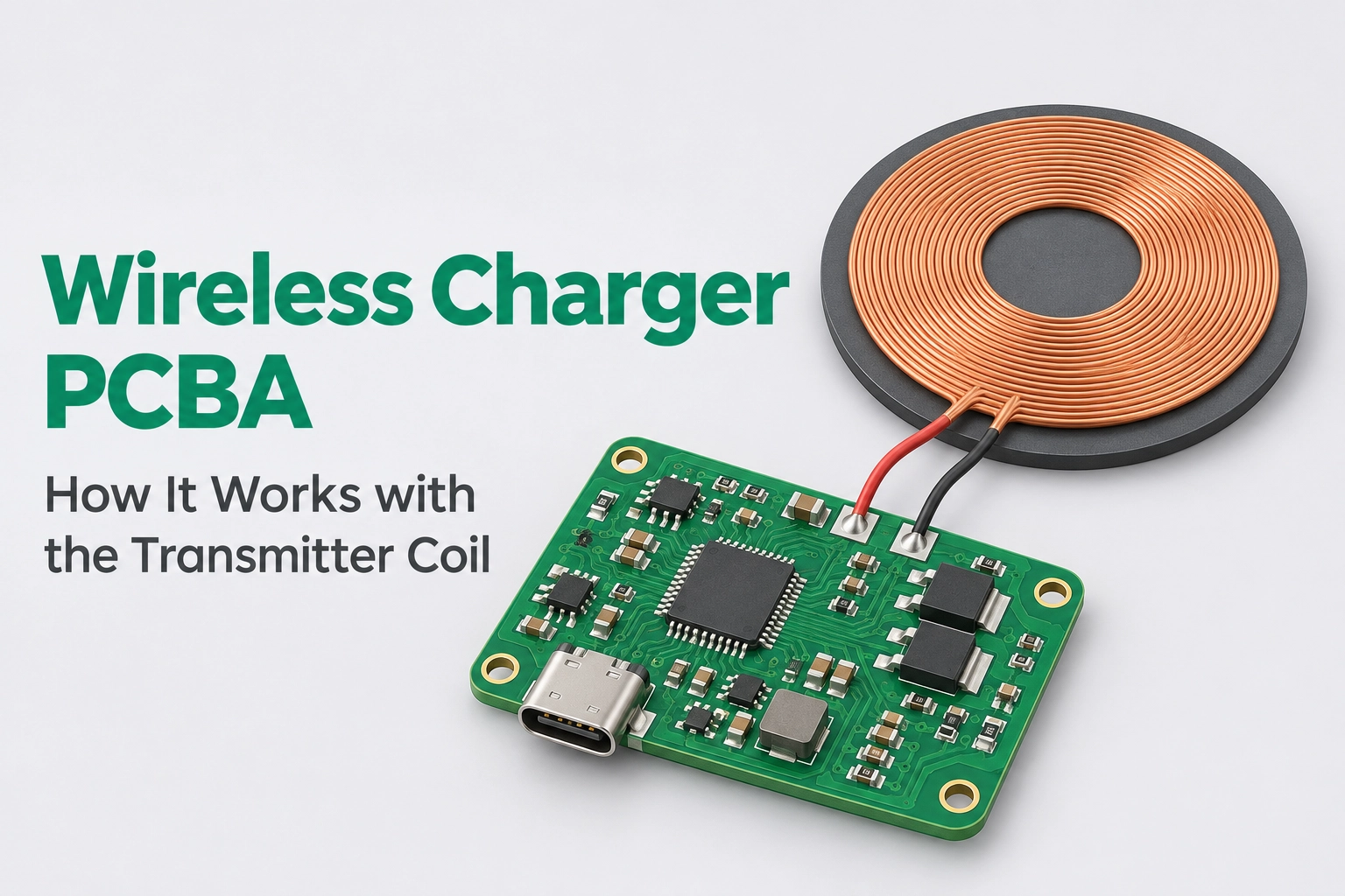
In an inductive wireless power system, the
printed circuit board assembly (PCBA) and the magnetic coil function as a
coupled high-frequency power stage. The wireless charger PCBA regulates rail
voltage, executes firmware control loops, and drives alternating current
through the coil to generate the dynamic magnetic flux required for power
transfer.
For hardware engineers and manufacturing teams,
achieving high system efficiency and yield requires attention to both circuit
topology and physical layout. How the wireless charging transmitter board
connects, aligns, and interacts with the physical coil directly affects
coupling coefficients, operating temperatures, and EMI behavior.
This guide explains the power drive
architecture, component selection checks before production, mechanical mounting
practices for enclosure integration, and post-assembly power and thermal test
methods.
How a Wireless Charger Transmitter Board Works
A wireless charging transmitter board converts
incoming direct current (DC) into a high-frequency alternating magnetic field.
This field spans the gap between the base station and the target receiver coil.
Power
Conversion Sequence
1. Input Rail Negotiation:
The power management stage accepts DC input
(such as 5V, 9V, 12V, or 20V) through a USB Type-C connector or a dedicated DC input,
depending on the design. The onboard USB PD controller manages handshakes with
the power source to set the voltage rail in USB PD-enabled designs.
2. Inversion Stage:
A half-bridge or full-bridge MOSFET inverter
converts the DC voltage rail into high-frequency AC current. Some conventional Qi-compatible
inductive transmitters typically switch within the 110 kHz to 205 kHz band,
while Qi2 MPP transmitters operate at 360 kHz.
3. Resonant Drive & Flux Generation:
The AC current drives an LC resonant tank made
of tuned resonant capacitors and the connected wireless charging transmitter
coil. The active AC current through the primary coil induces high-frequency
magnetic flux. When a secondary receiver coil enters this field, mutual
inductance transfers energy across the air gap.
During active power transfer, the driver MCU
tracks phase shifts, current draw, and back-scattered amplitude modulation
signals from the receiver. It continually adjusts switching frequency, duty
cycle, or input voltage to maintain target power levels.

Key Components of a Wireless Charger PCBA
Checking board components and coil
sub-assemblies prior to final mounting reduces assembly defects and subsequent troubleshooting.
|
Subsystem
/ Component
|
Technical
Function
|
Pre-Production
Inspection & Vendor Checks
|
|
Main Logic Controller (MCU / ASIC)
|
Runs control loops, signal
modulation/demodulation, and fault protection
|
Check firmware build version, correct
manufacturer part number (MPN), and package pin-1 marking and orientation in
the carrier tape
|
|
MOSFET Power Stage
|
Switches DC rail voltage into high-frequency
AC current
|
Confirm low RDS(on) parts against
the AVL; verify solder paste stencils to prevent solder bridging
|
|
Resonant Capacitors
|
Form the LC resonant tank paired with the
transmitter coil
|
Require C0G/NPO dielectric grade MLCCs; check
±5% capacitance tolerance to prevent tuning shifts
|
|
Transmitter Coil Assembly
|
Converts AC drive current into high-frequency
magnetic flux
|
Check Litz wire strand count, DC resistance
(DCR), inductance (L), and lead tinning quality
|
|
Ferrite Shielding Plate
|
Guides magnetic flux lines and isolates
underlying electronics
|
Inspect ferrite backing for cracks, verify
magnetic permeability specs, and check tape adhesion
|
|
Demodulation & Current Sensing
|
Decodes incoming communication packets from
the receiver
|
Check precision op-amp ratings and
current-sense resistor tolerance (±1% or tighter)
|
At PCBasic, incoming quality control (IQC)
checks component identity and condition against approved project documentation
before assembly. SPI, AOI, and X-ray inspection, where applicable, help verify
assembly quality, while electrical and functional tests follow the agreed
project requirements.
Practical
Component Notes
• Capacitor Class Selection: Standard MLCCs with X7R or X5R
dielectrics drop significant capacitance under DC bias and temperature swings.
High-Q C0G/NP0 capacitors are commonly used in the LC tank to keep resonant
frequency stable under continuous AC ripple current.
• Coil and Ferrite Inspection: The coil winding uses multi-strand
Litz wire to minimize skin effect losses at the transmitter’s operating
frequency. Check lead ends for complete solder tinning. Hairline fractures in
the ferrite shield alter coil inductance and create localized hot spots during
full-power operation.
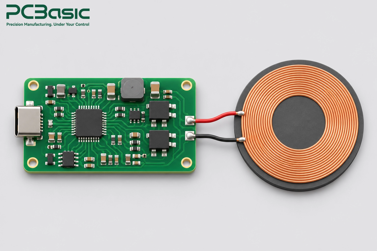
Matching the Board and Coil to the Charging Pad
A Qi wireless charger PCBA must be electrically
matched to its target coil assembly. Because the coil acts as the primary
winding of a loosely coupled transformer, system operation depends on key
electrical characteristics:
• Inductance and Resonant
Tuning: Some
commercial transmitter coils typically range from 6.3 μH to 24 μH. The
capacitor array on the board must match this primary coil inductance to set the
nominal LC resonant frequency:
f_r = 1 / (2 × π ×
√(L × C))
• Ferrite Backing Function: The ferrite sheet behind the
winding pulls magnetic flux upward toward the target device and reduces
magnetic coupling from reaching the wireless charger PCB assembly below.
Inadequate shielding allows stray flux to induce eddy currents in PCB copper
pours, raising temperatures and draining efficiency.
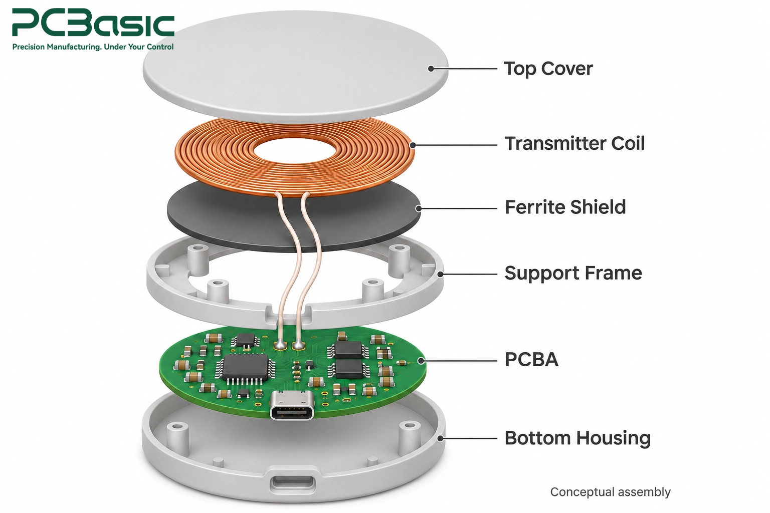
Assembling the Board, Coil, and Enclosure
Integrating a tested PCBA and coil into a physical housing requires careful control over component
placement and stack-up height.
Mechanical
Stack-Up Order
1. Top Housing: Non-metallic outer surface (e.g., ABS, PC, or
glass).
2. Transmitter Coil: Litz winding fitted flush against
the inside of the top cover.
3. Ferrite Shield: Fixed directly against the bottom face of the
coil.
4. Spacer / Mechanical Frame: Non-conductive structural support
frame.
5. Main Board: Wireless charger PCBA mounted with
thermal interface material (TIM) bridging heat paths down toward the lower
enclosure base.
Assembly
Guidelines for Production
Assembly teams should distinguish between
static component placement inside the housing and dynamic receiver alignment
during operation:
• Transmitter Coil Placement
(Internal Mounting): This step refers to securing the coil module inside the housing base.
Mount the coil against mechanical locating pins or molded alignment ribs as
specified in engineering drawings. Press double-sided tape onto the ferrite
sheet flat to prevent air pockets that trap heat.
• Wire Lead Routing: Lead wires running from the coil to
the board must not be strained or pinched under internal housing ribs. Pinched
leads can break individual Litz wire strands or damage the insulation and cause
short circuits when closing the housing.
• Post-Enclosure Inspection: After snapping or screwing the
enclosure halves together, check that the internal coil has not rotated or
drifted relative to top housing alignment markings.
• Wireless Charging Coil
Alignment (External Operation): This refers to the positioning of the external
device receiver coil relative to the internal transmitter coil. Keeping the
vertical air gap across the top housing wall within design limits maintains the
coupling coefficient (k) and minimizes power loss.
Testing Charging Power and Temperature After Assembly
Performance limits and thermal rise depend
heavily on enclosure plastics, internal air gaps, and board placement.
Validation testing should evaluate assembled units against a calibrated
reference receiver (Test RX) using a clean DC supply.
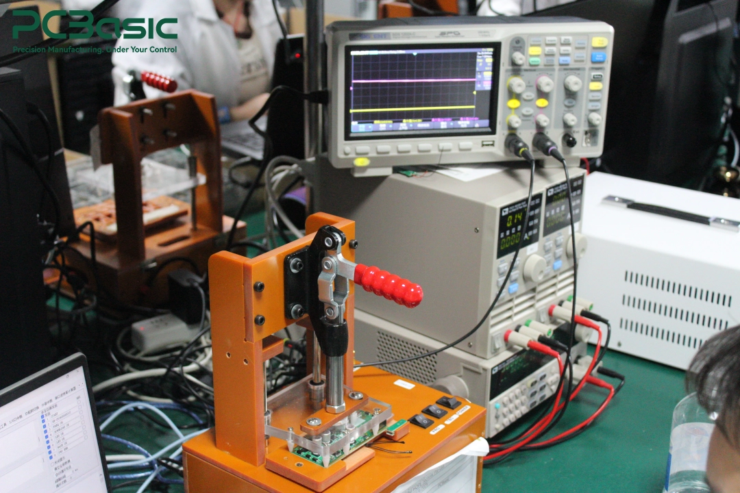
Functional
Testing Method
To test an assembled unit, connect a regulated
DC supply to the charger input. Position a standardized reference receiver on
the active charging surface and connect its DC output to an adjustable
electronic load.
1. DC-to-DC Efficiency Measurements: Calculate power efficiency by
measuring DC input power (Pin =Vin ×Iin)
against DC output power delivered by the reference receiver to the load (Pout =Vout ×Iout):
Efficiency =Pout/Pin ×100%
Compare efficiency readings before and after
housing assembly to confirm that enclosure materials or internal misalignments
do not introduce parasitic losses.
2. Foreign Object Detection (FOD) Steps: FOD verification includes two main
checks:
• Pre-Power Transfer Detection: Prior to delivering full power, the
driver controller measures LC tank parameters (such as Q-factor shifts or
frequency offsets) to identify metal debris on the pad surface.
• In-Band Power Loss
Monitoring: During power delivery, the board calculates a power difference (ΔP=Ptransmitted -Preceived_reported) and accounts for expected losses and
measurement uncertainty through calibration. Metal placed on the pad can
develop eddy currents, driving up ΔP. The controller must detect excess loss
above the applicable threshold and safely cut power or reduce drive current.
3. Thermal Profiling: Run full-load thermal tests in an
environmental chamber or a temperature-controlled room. Measure temperatures
using thermocouples placed on the MOSFET pads, resonant capacitors, coil wire,
and upper housing surface. Confirm that surface temperatures stay within target
thresholds without triggering internal MCU thermal throttling.

Conclusion
Designing a reliable wireless charging system
requires balancing electrical tuning with consistent factory assembly. Matching
the wireless charger PCBA to a verified transmitter coil helps achieve high
transfer efficiency, stable thermal performance, and dependable field
operation.
By strictly verifying components before
mounting, controlling coil placement during housing assembly, and executing
calibrated DC-to-DC load testing, engineering and manufacturing teams can build
robust products at scale.
For your wireless
charger PCBA project, PCBasic can review the BOM, Gerber files, coil
specifications, and test requirements to help define the assembly and
inspection scope. Contact our team to discuss component
sourcing, PCB assembly, and final product assembly for your project.
FAQs
Q1: How do I choose between a single-coil and a
multi-coil transmitter layout?
Select a single-coil layout for cradles or
docks where device placement is fixed. Multi-coil arrays use switching matrices
to expand the active charging area on flat pads, but they increase circuit
complexity, board area, and overall component costs.
Q2: Why is ferrite backing selection critical
for transmitter coils?
The ferrite sheet concentrates magnetic flux
toward the receiver coil and shields the underlying circuit board. Effective
ferrite shielding prevents magnetic fields from generating eddy currents in
copper pours, which would lower efficiency and produce excessive heat.
Q3: What causes excessive heat in an assembled
wireless charger?
High temperatures are generally caused by high
coil wire DC resistance (DCR), conduction losses in high- RDS(on) switching
MOSFETs, or large receiver-to-transmitter separation gaps that force higher
driving currents. Using low-DCR Litz wire coils, efficient MOSFET switches, and
thermal interface materials helps dissipate heat through the bottom enclosure.
Q4: Can I pair any standard coil with my
wireless charger board?
No. The coil’s inductance (L) and
quality factor (Q) must meet the board’s design requirements, with L
matched to the resonant capacitor values. Connecting an unmatched coil shifts
the resonant frequency, lowering transfer efficiency or causing the controller
to fault during power negotiation.