Global high-mix volume high-speed PCBA manufacturer
9:00 -18:00, Mon. - Fri. (GMT+8)
9:00 -12:00, Sat. (GMT+8)
(Except Chinese public holidays)
Global high-mix volume high-speed PCBA manufacturer
9:00 -18:00, Mon. - Fri. (GMT+8)
9:00 -12:00, Sat. (GMT+8)
(Except Chinese public holidays)
HomePage > Blog > Knowledge Base > HDI Boards | High-Density Interconnect Printed Circuit Boards (PCBs)
In the present day, we can see how printed circuit boards (PCBs) have immensely helped technology advancement, with HDI boards being the most advanced. HDI boards have become more necessary as technology trends demand smaller, faster, and more accurate tools. There has been high deployment of HDI circuit boards in consumer electronics, telecommunication, and other sectors as there is an increased need for smaller end products.
This article will cover the HDI PCB definition, structure, and application. Also, understanding the pros and cons of utilizing HDI PCBs and the reason why HDI technology is required in today's electronic world is significant.
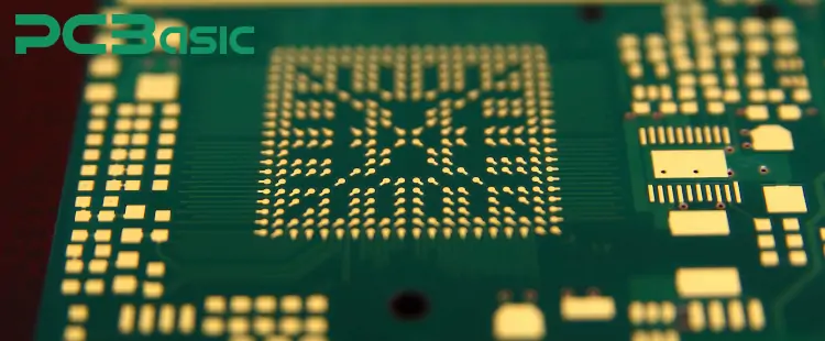
HDI boards belong to the category of printed circuit boards (PCBs) that have higher component density and finer lines. These boards incorporate microvias, blind and buried vias, and relatively thin traces to give better performance. With the advancement of technology, HDI PCBs have also become increasingly important because of the majority of electronic devices nowadays, such as mobile phones, portable computers and wearable technologies.
High-density interconnect boards are the preferred option because they allow the addition of more components in the clamped size for best signal transmission, no signal loss, and better operational efficiency, which is excellent for high-frequency multilayer designs.
HDI PCBs are designed with specific structures that enhance their functionality and capacity to handle complex designs. The common structures used in HDI boards are:

This basic HDI structure consists of a single layer of high-density interconnect on both sides of a core layer. It's often used for simple designs where only a few layers are necessary.

The 2+N+2 structure has two HDI layers on both sides of the core layer, allowing for more interconnections and greater design complexity. This structure is favored for more advanced electronics where higher component density is required.
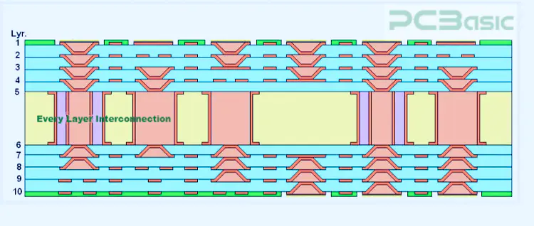
The ELIC structure is used in highly sophisticated designs where every layer of the PCB is interconnected. This type of HDI PCB provides optimal electrical performance, making it suitable for high-end electronics such as smartphones and medical devices.
Vias are small holes in HDI PCBs that allow electrical connections between different layers. HDI circuit boards utilize various vias to maximize space and enhance performance.
Microvias
Microvias are tiny vias that are typically less than 100 microns in diameter with the latest technology. They are crucial for HDI boards as they provide the high-density connections necessary for complex designs.
Blind and Buried Vias
Blind vias connect the outer layer to one or more inner layers, while buried vias connect only inner layers, without reaching the outer surface. Both types are widely used in HDI PCBs to save space and improve the board's performance.
Capped Vias
In some cases, vias are capped with a conductive material to ensure better reliability and prevent contamination. Capped vias are frequently used in high-density interconnect PCBs to enhance durability.
Higher Component Density
The most important benefit of HDI PCBs is the capability to have higher component density. Since microvias, blind and buried vias, and fine line traces can be incorporated by HDI boards to get more connections within much smaller space.
With HDI circuit boards, increasingly complex systems come in ever-decreasing footprints, this miniaturization being a key requirement for contemporary consumer electronics that includes smartphones, tablets, and wearables.
Improved Electrical Performance
Another important advantage of HDI boards is improved electrical performance, resulting from the use of advanced vias plus ultra-fine traces. The reduced distances between components plus optimized routing paths have all been designed to minimize signal interference and electrical noise. This method has been explicitly used to ensure enhanced signal integrity, which basically stands very critical for high-speed application use, cases including data communication and computing devices where even slight delays or losses could greatly affect performance.
Reduced Weight and Size
The miniaturization of electronic components made possible by HDI PCBs directly leads to lighter and smaller devices. Such fast become vital for industries like consumer electronics, medical technology and aerospace, in which portability and diminished proportions are central.
While HDI PCBs offer many benefits, they also come with certain limitations.
Higher Manufacturing Costs
Despite many technical advantages, one of the major drawbacks of HDI PCBs is their superior manufacturing costs. HDI boards require advanced technology like laser drilling for microvias, sequential lamination and more precise imaging techniques with specialized equipment and skills. Its advanced processes result in a higher total cost of production.
Furthermore, the functionality of high-performance materials, such as thin laminates and exotic surface finishes used in HDI PCB manufacturing also adds to the cost. These higher manufacturing costs could be a limiting factor for companies operating on tight budgets or in high-volume production runs.
Complexity in Design and Production
The HDI PCB Design and manufacturing is very challenging compared to the standard size PCBs. It takes seasoned engineers and designers to design HDI PCBs. And the complexity extends beyond managing two layers of interconnects and perfectly aligned vias and traces. These kinds of intricate designs require accurate engineering, which can be more time-consuming and error-prone if not managed properly throughout the design cycle.
More significantly, the requirement of sophisticated fabrication methods such as sequential lamination introduces problems in terms of mass production due to its precise control on each step of manufacturing procedures.
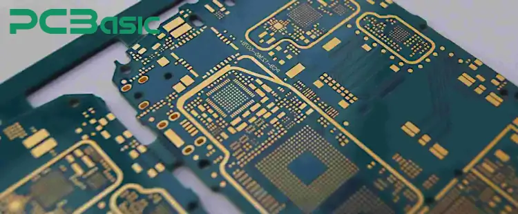
The manufacturing process for HDI boards is highly specialized, involving advanced techniques such as laser drilling, microvia formation, and sequential lamination. The process typically includes:
1. Design and Layering: A detailed design is created, specifying the placement of microvias, blind and buried vias, and component density.
2. Drilling and Via Creation: Laser drilling is used to form microvias, which are then plated to ensure reliable connections between layers.
3. Lamination and Assembly: The layers of the PCB are laminated together using heat and pressure, followed by component placement and soldering.
HDI boards are used across a wide range of industries due to their advanced capabilities. Like:
· Consumer Electronics: Smartphones, tablets, and wearable devices all rely on HDI circuit boards to deliver high performance in a compact design.
· Telecommunications: High-density interconnect PCBs are widely used in telecommunications infrastructure, including network switches and routers, where high signal integrity is critical.
· Medical Devices: In the medical field, HDI PCBs enable the miniaturization of complex diagnostic and monitoring equipment, making them more portable and efficient.
HDI PCBs address the growing need for more compact, lightweight, and potent devices, and they constitute a major breakthrough in the world of electronics. Although they have drawbacks, like increased production costs and design complexity, their advantages make them a desirable option for high-performance applications. If you want to buy HDI boards, you can come to PCBasic. At PCBasic, we specialize in the design and manufacture of HDI PCBs to meet the unique needs of our clients. Our state-of-the-art facilities and experienced engineers ensure that we deliver high-quality HDI circuit boards tailored to your project's specifications. Whether you need a basic 1+N+1 structure or a complex ELIC design, we have the expertise to provide you with reliable and efficient solutions.
 About PCBasic
Time is money in your projects – and PCBasic gets it. PCBasic is a PCB assembly company that delivers fast, flawless results every time. Our comprehensive PCB assembly services include expert engineering support at every step, ensuring top quality in every board. As a leading PCB assembly manufacturer, we provide a one-stop solution that streamlines your supply chain. Partner with our advanced PCB prototype factory for quick turnarounds and superior results you can trust.
What is the difference between traditional PCBs and HDI PCBs?
The primary difference lies in the complexity and component density. HDI PCBs utilize advanced manufacturing techniques to incorporate more components in a smaller area, whereas traditional PCBs have a simpler design with fewer interconnections.
What industries benefit the most from HDI PCBs?
Industries such as consumer electronics, telecommunications, and medical devices benefit greatly from the use of HDI circuit boards due to their need for miniaturization and high performance.
How does the manufacturing process of HDI PCBs differ from standard PCBs?
The manufacturing process for HDI boards involves more advanced techniques, such as laser drilling and microvia formation, to achieve higher component density and improved electrical performance.
Assembly Enquiry
Instant Quote
Phone contact

+86-755-27218592
In addition, we've prepared a Help Center. We recommend checking it before reaching out, as your question and its answer may already be clearly explained there.
Wechat Support

In addition, we've prepared a Help Center. We recommend checking it before reaching out, as your question and its answer may already be clearly explained there.
WhatsApp Support

In addition, we've prepared a Help Center. We recommend checking it before reaching out, as your question and its answer may already be clearly explained there.