Global high-mix volume high-speed PCBA manufacturer
9:00 -18:00, Mon. - Fri. (GMT+8)
9:00 -12:00, Sat. (GMT+8)
(Except Chinese public holidays)
Global high-mix volume high-speed PCBA manufacturer
9:00 -18:00, Mon. - Fri. (GMT+8)
9:00 -12:00, Sat. (GMT+8)
(Except Chinese public holidays)
HomePage > Blog > Knowledge Base > What is Copper Thieving in PCBs?
Copper plays a crucial role in circuit boards, including conductivity, heat dissipation, current carrying and enhancing circuit stability. Therefore, in the manufacturing process of a circuit board, the manufacturers pay particular attention to the copper on the circuit board. In addition to thickness and weight, the distribution of copper also has a huge impact on product quality. Uneven copper distribution may lead to PCB warping, uneven plating, and electrical instability.
Copper thieving is a method commonly used by PCB manufacturers to solve the problem of uneven copper distribution. In this article, we will explore what copper thieving in PCBs is, why it’s needed, the different meanings of varying thieving point sizes, and how this process improves PCB quality.
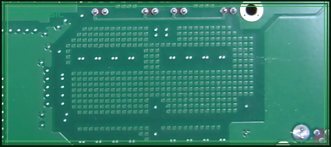
Copper thieving is a commonly used layout technique in PCB manufacturing used to solve the problem of uneven copper distribution on the circuit board. By adding some small, non-functional copper on the board where there are few or no components and the copper distribution with high component density to balance high copper density. Copper thieving does not do the function in the circuit, transmit signals or participate in the circuit connection, but only balances the copper distribution on the board, thereby improving the manufacturing quality and structural stability.

As mentioned earlier, copper thieving is a technique to solve the problem of uneven distribution of copper on a circuit board. Affected by the design of the circuit board and the layout of the components, the copper distribution on the board is not very uniform: the copper density is higher in the place where the components are densely assembled, and lower in the place where the components are less. Therefore, the problem of uneven distribution of copper layers on a plate is formed.
By adding non-functional copper shapes in low-density areas, copper thieving helps balance the copper distribution. Therefore, to answer the question “Why Do We Use Copper Thieving in PCBs?” is essentially to explain the benefits of uniform copper distribution.
1. A circuit board with an even distribution of copper can prevent warping and deformation.
During the manufacturing process, PCBs undergo multiple heating and cooling cycles. If the copper distribution on both sides or across different layers of the board is uneven, thermal expansion and contraction will also be different, which may cause one side to experience more tension than the other, leading to warping. Copper thieving technology balances copper density to make copper distribution more uniform, thereby reducing thermal expansion differences, maintaining board flatness, and preventing warping.
2. A circuit board with an even distribution of copper can improve plating quality.
Electroplating is an important technology in circuit board manufacturing. During the plating process, an electric current flows through the PCB, depositing copper on its surface. We all know that the current always prefers to flow to where the resistance is low, that is, where the copper density is high. Therefore, if the distribution of copper on the circuit board is uneven, it will lead to different current flowing through the board, which will affect the plating quality. Where copper is distributed more, the plating layer is thicker, and low, the plating layer is thinner, resulting in inconsistent plating quality. Copper thieving effectively solves this problem, ensuring higher quality and reliability of the PCB.
3. A circuit board with an even distribution of copper can enhance circuit signal integrity.
The integrity of the signal is very important for the circuit board, especially in the high-frequency circuit board. Empty areas on the board where no components are mounted, with little or no copper distribution, may accumulate static electricity, which can interfere with signal transmission and even damage components. Copper thieving addresses this by adding copper to these blank areas, providing a stable and balanced environment for circuit transmission. This reduces the risk of static buildup and helps maintain signal integrity on the PCB.
4. A circuit board with an even distribution of copper can optimize the etching process.
Etching is a key step in PCB manufacturing in which unwanted copper layers are removed by a chemical solution. If the copper distribution of the PCB is not uniform, there may be excessive or insufficient etching problems during the etching process, which affects the final conductive graphic accuracy. Copper thieving technology makes the copper distribution more uniform, ensures the stability of the etching process, and improves the quality of the PCB.
Although copper thieving is not used in all PCBs, it plays a crucial role in certain applications and industries.
|
PCB Types |
Roles of Copper Thieving |
|
High-Frequency PCB |
Prevents static buildup and signal interference, enhancing signal quality. |
|
Multilayer PCB |
Balances copper distribution across layers, ensuring uniform thermal stress and preventing delamination. |
|
High-Density Interconnect (HDI) PCB |
Improves manufacturing precision, reducing defects and rework due to uneven copper distribution. |
|
Large-Size PCB |
Mitigates warping issues caused by uneven copper distribution over large areas. |
Observing different circuit boards carefully, we can find that the sizes or locations of the copper thieving is always inconsistent. This is because the size and location of it are determined by a variety of factors.
First of all, the size and position of the copper thieving are affected by the components. Copper thieving is non-functional and must be placed in an area that will not interfere with the actual circuit. Smaller copper thieving may be used in areas close to functional wiring or components to ensure that they do not accidentally connect or interfere with the circuit. Larger copper thieving can be placed in a completely blank area of the board to avoid interference.
Second, the copper thieving is affected by the density of the copper distribution on the circuit board. Areas with less copper density may need a larger copper thieving to compensate, while areas with higher copper density only need a smaller copper thieving to achieve balance.
And finally, the size and position of the copper thieving may also be adjusted according to the requirements of manufacturers, and the size and position requirements of the copper thieving are also adjusted by different PCB manufacturers or due to different production materials and equipment.
Copper thieving technology plays a crucial role in the PCB manufacturing process, balancing the copper distribution on a circuit board by adding non-functional copper, reducing product defects and improving product quality. Let us look forward to copper thieving continuing to play an important role in the future PCB design in promoting the development and progress of electronic manufacturing technology.

Assembly Enquiry
Instant Quote
Phone contact

+86-755-27218592
In addition, we've prepared a Help Center. We recommend checking it before reaching out, as your question and its answer may already be clearly explained there.
Wechat Support

In addition, we've prepared a Help Center. We recommend checking it before reaching out, as your question and its answer may already be clearly explained there.
WhatsApp Support

In addition, we've prepared a Help Center. We recommend checking it before reaching out, as your question and its answer may already be clearly explained there.