Global high-mix volume high-speed PCBA manufacturer
9:00 -18:00, Mon. - Fri. (GMT+8)
9:00 -12:00, Sat. (GMT+8)
(Except Chinese public holidays)
Global high-mix volume high-speed PCBA manufacturer
9:00 -18:00, Mon. - Fri. (GMT+8)
9:00 -12:00, Sat. (GMT+8)
(Except Chinese public holidays)
In PCB design, the differences between tenting vias, plugged vias with solder mask, and vias not covered often cause confusion. Many designers easily mix them up, leading to difficulties in fully utilizing the advantages of these processes. In this article, PCBasic will explain these concepts in detail, helping you accurately and clearly specify your design requirements when submitting PCB files for manufacturing.
A via is a small hole in a printed circuit board (PCB) used to connect electrical traces between different layers. By establishing electrical connections between the layers of the board, vias enable signals to transmit between them. Since vias are not used for mounting component leads, their hole and pad diameters are typically smaller.
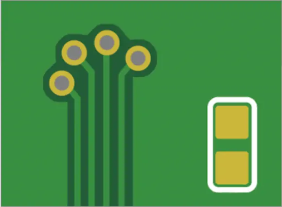
Tenting vias is one of the most popular and mature processes in PCB manufacturing. The “ink” in tenting vias refers to solder mask ink, and tenting vias means covering the via pad with this solder mask ink. The main purpose of tenting vias is insulation, so it is essential to ensure that the solder mask fully covers the pad and is thick enough. This prevents solder from adhering to the vias during surface-mount or through-hole component installation.
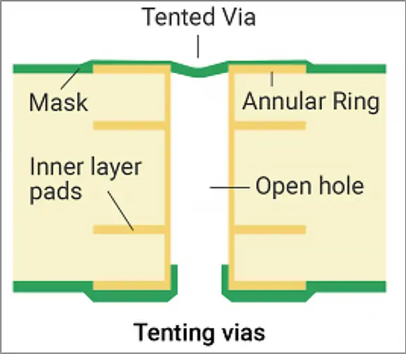

Note:
If your design file is in PADS or Protel format, please carefully check whether the through-holes for components are categorized as vias when requesting tenting vias from PCBasic. If they are, the component through-holes will be covered with solder mask, making them impossible to solder.
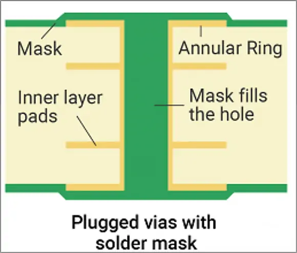
Plugged vias with solder mask involve using an aluminum sheet to fill the vias with solder mask ink during PCB production, followed by applying solder mask to the entire board. This ensures that all vias are completely opaque.
The purpose of this process is to block the vias to prevent solder balls from getting trapped inside. Solder balls can melt at high temperatures and flow onto the pads, causing short circuits, especially under BGAs (Ball Grid Arrays).
If the vias are not properly filled with solder mask ink, the edges of the holes may appear red, resulting in a defect known as false copper exposure. Poor via plugging can also negatively affect the appearance and quality of the PCB.
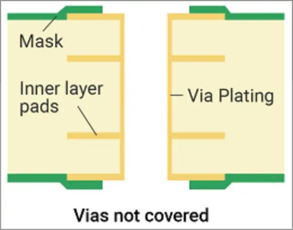

Vias not covered, also known as vias with solder mask opening, is the opposite of tenting vias—neither the via holes nor the pads are covered with solder mask.
This process increases the heat dissipation area, which is beneficial for thermal management. Therefore, if your PCB has high thermal requirements, you can choose vias with solder mask opening.
Additionally, if you need to use a multimeter to perform measurements on the vias, this process is also necessary.
However, vias with solder mask opening have a potential risk of solder bridging and short circuits, so design and manufacturing should be handled carefully.
Phone contact

+86-755-27218592
In addition, we've prepared a Help Center. We recommend checking it before reaching out, as your question and its answer may already be clearly explained there.
Wechat Support

In addition, we've prepared a Help Center. We recommend checking it before reaching out, as your question and its answer may already be clearly explained there.
WhatsApp Support

In addition, we've prepared a Help Center. We recommend checking it before reaching out, as your question and its answer may already be clearly explained there.