Global high-mix volume high-speed PCBA manufacturer
9:00 -18:00, Mon. - Fri. (GMT+8)
9:00 -12:00, Sat. (GMT+8)
(Except Chinese public holidays)
Global high-mix volume high-speed PCBA manufacturer
9:00 -18:00, Mon. - Fri. (GMT+8)
9:00 -12:00, Sat. (GMT+8)
(Except Chinese public holidays)
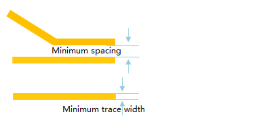
For rigid PCBs, it’s important to ensure that the minimum trace width and spacing comply with PCBasic’s manufacturing capabilities to guarantee both reliability and production yield. Please refer to the following specifications before submitting your design files.
The Minimum Track/Spacing for Outer Layer (Before Compensation)
|
Copper Weight |
Normal Process |
Medium Difficulty |
High Difficulty |
|
1 oz |
≥ 5/6 mil |
≥ 5/5 mil |
< 4/4 mil |
|
2 oz |
≥ 7/8 mil |
≥ 6/7 mil |
< 5/6 mil |
|
3 oz |
≥ 10/12 mil |
≥ 8/10 mil |
< 6/9 mil |
The Minimum Track/Spacing for Inner Layer (Before Compensation)
|
Copper Weight |
Normal Process |
Medium Difficulty |
High Difficulty |
|
1 oz |
≥ 4/5 mil |
≥ 4/4 mil |
< 3.5/4 mil |
|
2 oz |
≥ 6/8 mil |
≥ 6/7 mil |
< 5/6 mil |
|
3 oz |
≥ 8/11 mil |
≥ 8/10 mil |
< 6/9 mil |

Note:
At PCBasic, we strongly recommend designing your trace width and spacing to be above 6 mil (0.15 mm) whenever possible. This not only helps reduce manufacturing costs but also improves yield and process stability, especially for large-scale or high-layer-count PCB production.
Phone contact

+86-755-27218592
In addition, we've prepared a Help Center. We recommend checking it before reaching out, as your question and its answer may already be clearly explained there.
Wechat Support

In addition, we've prepared a Help Center. We recommend checking it before reaching out, as your question and its answer may already be clearly explained there.
WhatsApp Support

In addition, we've prepared a Help Center. We recommend checking it before reaching out, as your question and its answer may already be clearly explained there.