Global high-mix volume high-speed PCBA manufacturer
9:00 -18:00, Mon. - Fri. (GMT+8)
9:00 -12:00, Sat. (GMT+8)
(Except Chinese public holidays)
Global high-mix volume high-speed PCBA manufacturer
9:00 -18:00, Mon. - Fri. (GMT+8)
9:00 -12:00, Sat. (GMT+8)
(Except Chinese public holidays)
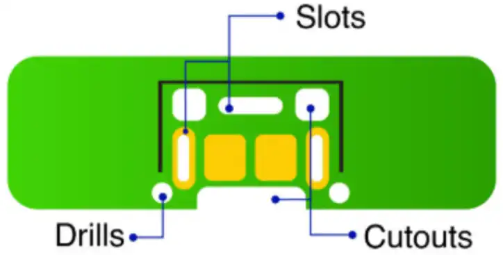
Sometimes, customers notice that cutouts or slots are missing from their finished PCB design data during engineering review. This usually happens because the cutout or slot shapes were drawn on the silkscreen layer instead of the proper mechanical or outline layers.
When the slot information appears in the silkscreen layer, our engineers may interpret it as text frames or graphic markings, rather than actual milling paths — leading to these features being overlooked during CAM processing.
To prevent such issues, PCBasic strongly recommends that all cutouts, slots, or milling contours be designed in the following layers:
• Outline layer (GKO or GML)
• Mechanical layer
• Drill layer (for plated slots or special hole shapes)
By placing cutout designs in the correct layer, you ensure accurate board contour machining, faster engineering confirmation, and a smoother production process at PCBasic.

Phone contact

+86-755-27218592
In addition, we've prepared a Help Center. We recommend checking it before reaching out, as your question and its answer may already be clearly explained there.
Wechat Support

In addition, we've prepared a Help Center. We recommend checking it before reaching out, as your question and its answer may already be clearly explained there.
WhatsApp Support

In addition, we've prepared a Help Center. We recommend checking it before reaching out, as your question and its answer may already be clearly explained there.