
Global high-mix volume high-speed PCBA manufacturer
9:00 -18:00, Mon. - Fri. (GMT+8)
9:00 -12:00, Sat. (GMT+8)
(Except Chinese public holidays)





HomePage > Blog > Knowledge Base > What Does PCBA Stand for in Electronics? Printed Circuit Board Assembly Explained
Table of Contents
1. What PCBA Means and Where the Term Stops
2. From Design Files to a Buildable PCBA
3. How PCBA Manufacturing Turns Data Into Hardware
4. Inspection and Testing Answer Different Questions
If an RFQ only says “PCB”, should the supplier quote for bare boards, or should they include component sourcing and assembly as well? If this boundary is not clearly defined in advance, the two sides can easily discuss different deliverables from the beginning. The problem often lies not in the lack of understanding of the product by both parties, but in the unclear delivery boundary between PCB and PCBA.
PCBA stands for Printed Circuit Board Assembly, while PCB stands for Printed Circuit Board. In simple terms, PCB usually refers to the manufactured bare board that has not yet installed components, while PCBA is the circuit board after the specified components have been assembled on the PCB. In actual projects, this distinction will directly affect the scope of materials, production documents, testing requirements, quotation content, and the final deliverables.
For the hardware team or the procurement team, understanding what PCBA represents in actual manufacturing is more meaningful than simply memorizing this abbreviation. In addition to "What is PCBA?" the practical question is "What kind of physical deliverables do we expect to obtain, and what information is needed to define it?"
When the project involves PCB manufacturing, component procurement, PCBA assembly, functional testing, Box Build or wiring harness processing, the consistency of information among different manufacturing stages is equally important. In order to maintain consistency in the PCB version, BOM choices, and test requirements throughout the production, assembly, and verification phases, the PCBasic manufacturing platform may include these procedures into a single manufacturing flow. This lessens the possibility that design data, quotation content, real production, and final testing will all have different information.
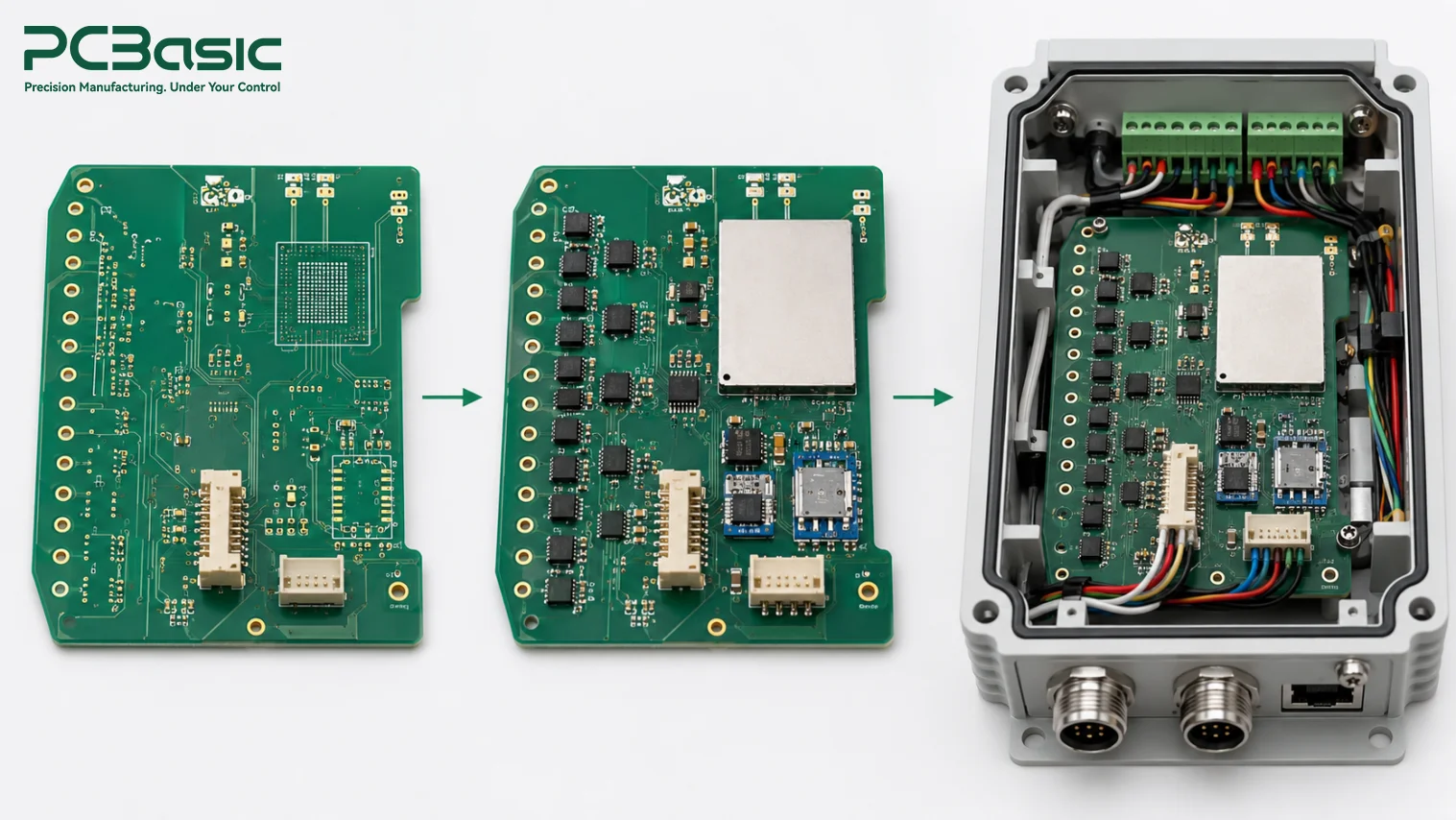
When does a PCB become a PCBA? It's quite simple. A PCB is a bare board that has been manufactured but has not yet had the components installed. Once resistors, capacitors, ICs, connectors, and other specified components are installed and soldered, it becomes a PCBA.
However, there is another confusing issue here: Does testing, program burning, anti-corrosion coating, and even casing assembly all fall under the PCBA category? The answer is not a blanket one. The key lies in the delivery scope agreed upon by both parties.
Once the PCBA is completed, does that mean the subsequent steps are automatically included? Actually, that's not necessarily the case. After mounting and soldering, the circuit board may still require programming, electrical inspection, functional testing, conformal coating, even cable connection, enclosure assembly and final system testing. All of these are additional deliverables that need to be confirmed. It's much more reliable to clearly state them in the quotation than to assume them both way.
|
Term |
What you receive |
Key files and requirements |
|
PCB |
Fabricated bare board without mounted components |
Gerber or ODB++, fabrication drawing, stack-up, material/finish, outline, panel requirements |
|
PCBA |
PCB with specified components assembled |
PCB files + BOM, pick-and-place data, assembly drawing, substitution rules, inspection/test requirements |
|
Integrated Assembly |
PCBA integrated with cables, enclosure, and other hardware |
PCBA files + harness/enclosure data, mechanical requirements, programming instructions, labels, final acceptance tests |
After looking at this table, it’s actually quite easy to tell the difference: a PCB is a bare board, while a PCBA is a board with components already assembled; only after that does the process move on to the integration of cables, enclosures, and the final assembly. A complete electronic device may contain one or more PCBAs, but a PCBA itself is not automatically the same as the final product.
The quotation contents for PCB and PCBA are not the same. The quotation for bare boards mainly covers the manufacturing costs of PCB such as laminate, copper thickness, drilling, plating, surface treatment and forming; while the quotation for PCBA also includes components, steel mesh or fixtures, assembly, welding, inspection, program burning or testing. The order quantity and expected yield rate risks will also affect the final price. Therefore, if the inquiry states “PCB” but the actual requirement is to complete the assembly into a PCBA, the initial quotation may miss important materials and processing costs.
Before sending an RFQ, clearly define what you expect to receive: a bare PCB, an assembled PCBA, a tested PCBA, or a completed box build. If testing is required, it is also necessary to specify exactly what "testing" entails. This way, when comparing the quotations from different suppliers, it will be possible to confirm that everyone is reporting the same set of deliverables, rather than having seemingly different prices while the actual scope of services provided also differs.
To truly turn the design files into a producible PCBA, Gerber files alone are not sufficient. Gerber files can only define the PCB itself, but they are not enough to explain how a PCBA should be assembled, what to assemble, and how to test it. You also need to provide the BOM, Pick-and-Place data, assembly drawings, and test requirements. The more complete the information is, the easier it is for the factory to complete the production as required.
Let's start with the bare board files. Usually, Gerber or ODB++ data, drill files, manufacturing drawings, as well as layering, materials, copper thickness, surface treatment, impedance control and panel assembly requirements need to be provided. At the same time, it is necessary to confirm that the same version is used for different files. If connectors, mounting holes or board edges need to be coordinated with the enclosure, it is best to directly mark the key dimensions instead of relying solely on screenshots for the factory to make the judgment.
After the bare board files are determined, it is necessary to clearly state the assembly requirements. This usually includes:
• BOM: Reference designators, manufacturer part numbers, values, packages, quantities, and explicit substitution rules
• Pick-and-Place Data: Component coordinates, surface location, and rotation angle.
• Assembly Drawing: Polarity, DNP position, special processing requirements, and components requiring manual insertion.
• Test Instructions: If functional testing is required, the input, load, interface, expected output, and passing standards should be defined in advance.
These documents do not merely need to be "prepared and ready"; what's more important is that they must be consistent with each other. For instance, if the version of the BOM and the assembly drawing are not in agreement, even if the board appears to be assembled normally, it may still result in an incorrect product. Therefore, for PCBA, the document version, material information, soldering data, and test requirements all need to be aligned to the same production version.
Once production begins, the key is to try to prevent problems from occurring before the assembly process. PCBasic's PCB assembly services will integrate the BOM and component management processes to inspect the materials before they are put into production. If there are any abnormalities in the part number, packaging, quantity, or substitute material, they can be confirmed first before proceeding to the subsequent assembly process.
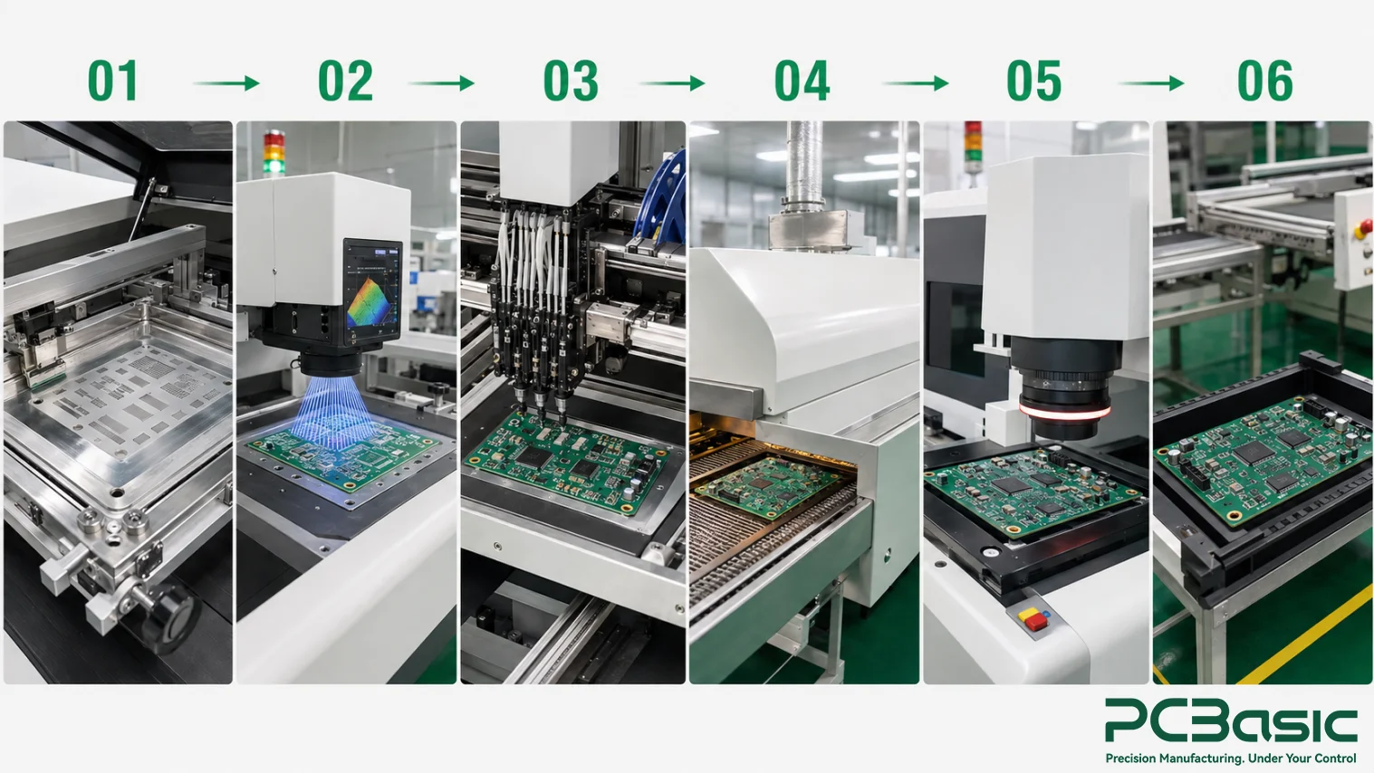
The data is ready, but this is only the first step. Once production begins, the key is to place the inspections at the locations where problems are most likely to occur, rather than waiting until the finished products are completed before looking for the reasons. Incoming materials, solder paste printing, component mounting, reflow soldering, and through-hole welding - each step can potentially affect the final outcome. Thus, if an anomaly occurs, it will be easier to determine whether the problem started at a certain stage or if the testing conditions were not clearly defined.
In SMT production, inspection does not wait until reflow is finished. PCBasic first checks the thickness, volume and position of the solder paste after the solder paste is printed through 3D SPI. After the components are mounted, it will conduct AOI before reflow soldering to confirm whether there are any missing parts, wrong parts, offsets or polarity problems. After the reflow soldering is completed, AOI is used to check the welding and component status. By placing the inspection after different processes, it becomes easier to determine whether the problem is caused by the printing, mounting or soldering stage.
If you want to gain a deeper understanding of the interrelationships among solder paste printing, placement, reflow soldering and inspection, you can continue to refer to the SMT assembly process. If there are fine-pitch components, BGA/QFN type bottom terminal packages, moisture-sensitive components, or if there are special directions or temperature resistance requirements, it is best to mention them in advance in the RFQ. Only in this way can the factory arrange the SMT process and inspection plan more accurately.
If there are through-hole components such as connectors, transformers, and relays on the board, then the SMT approach alone cannot be used. These components usually require manual insertion, wave soldering, selective soldering or local re-welding. Besides electrical connections, mechanical positioning is also crucial, such as whether the pins are inserted properly, whether the connectors are aligned, whether the soldering is sufficient, and whether high components will affect the subsequent shell assembly.
So, if your board is a mixture of SMT and through-hole components, it is best to mark these components separately in the assembly drawing. Which components need to be installed flat, which ones should be kept at a certain distance from the board, and which areas should not be subjected to wave soldering, all these should be clearly stated in advance. This gives the manufacturer a clear process route, rather than just making their own judgments based on the BOM.
Inspection and testing are not the same thing. Inspections such as SPI, AOI, and X-Ray mainly aim to find signs of defects left during the manufacturing process. Function tests, on the other hand, focus more on whether this PCBA can truly operate normally under the specified electrical and operational conditions. Therefore, a board passing an appearance inspection does not necessarily mean it will function properly under load; likewise, a simple power-on test not showing any problems does not mean there are no potential issues with the solder joints or connections. Some defects may only manifest themselves under conditions such as temperature changes, vibrations, or long-term use.
Different inspection equipment focus on different issues. SPI mainly checks the solder paste printing before assembly, while AOI is more suitable for inspecting the position, polarity and visible solder joints of components. For packaging like BGA where the solder joints are hidden at the bottom of the device, mere appearance inspection is not sufficient. At this point, X-Ray is usually needed to check for voids, bridging, insufficient solder or abnormal positions in the hidden solder joints. For such devices, you can also refer to PCBasic's BGA assembly capabilities to learn about the corresponding assembly and inspection methods.
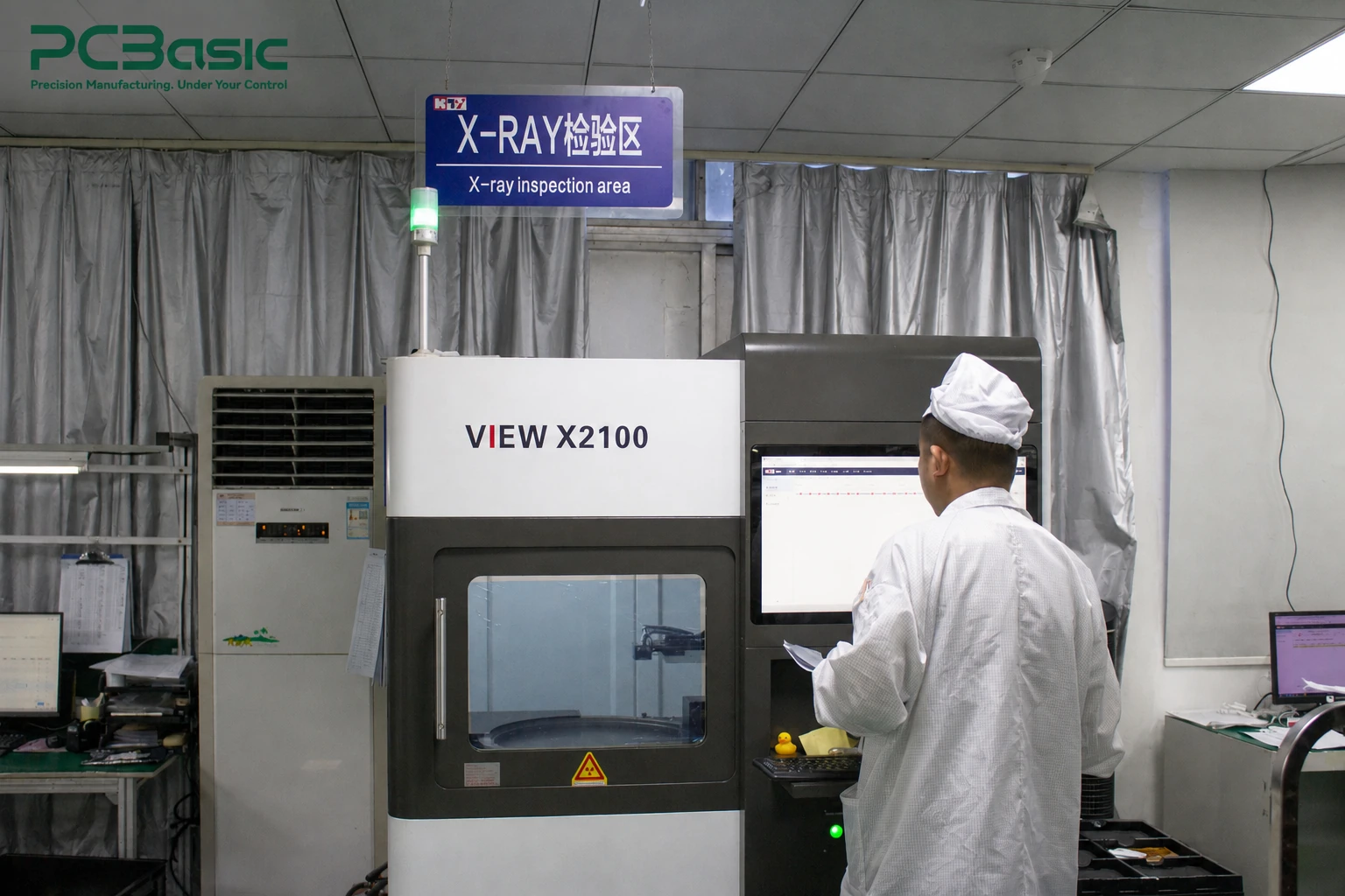
Therefore, when choosing the inspection method, the key point is not that the more equipment the better, but rather whether it can detect the defects that you are truly concerned about. For example, if there are hidden soldering points such as BGA and QFN on the board, you need to consider X-Ray and the corresponding acceptance standards in advance; while AOI mainly focuses on the appearance and assembly status, and cannot replace electrical or functional tests.
Just stating "functional testing is required" is not enough. You should at least explain the power supply conditions, input or simulated signals, load, the interfaces to be tested, the expected output, and what constitutes a pass. If this board needs to communicate with other modules, you should also specify in advance whether fixtures, gold samples, protocol descriptions, or supporting hardware will be provided during the test. The more clear the test conditions are, the easier it is for the supplier to accurately assess the labor hours, fixtures, and test plan.
The assembly and testing process of PCBasic can include visual inspection, functional testing, rework, and pre-shipping inspection. However, this process is contingent upon the customer clearly defining the criteria for pass and fail. Only in this way can the functional testing truly determine whether this PCBA meets the product requirements, rather than merely obtaining an ambiguous "pass" result.
In the end, differentiating between PCB and PCBA is not just about memorizing two different terms. What is truly important is to clearly define the scope of delivery: Do you need a bare PCB, a fully assembled PCBA, or a complete product that includes testing, programming, cable integration, and enclosure assembly? The clearer the boundaries, the less likely there will be deviations in subsequent quotations, production, and acceptance.
When preparing an RFQ, keep the PCB data, BOM, assembly requirements and test conditions in the same version, and clearly state the required delivery scope at one time. If the project also includes program burning, wiring harness, enclosure or Box Build, it should also be included in the RFQ in advance.
If you are still unsure whether the existing data is sufficient for production, or which assembly and testing procedures should be adopted, you can apply for a PCBA project review. PCBasic will assess the manufacturing and verification plans based on your actual delivery requirements.
Q1: What is the difference between PCB and PCBA?
A1: A PCB is the fabricated bare circuit board. A PCBA is that board after the specified components have been mounted and soldered. Programming, functional testing, cables, and an enclosure may be included in a broader order, but they should be stated separately rather than assumed.
Q2: What files are normally required for PCB assembly?
A2: A useful package includes the bare-board data, BOM, centroid or pick-and-place file, assembly drawings, polarity and do-not-fit notes, approved substitution rules, and any programming or test instructions. Keep revision identifiers consistent across all files.
Q3: Does a completed PCBA automatically include functional testing?
A3: No. Visual inspection, AOI, X-ray, electrical checks, and functional testing answer different questions. If functional testing is required, define the power, input, load, interface, expected output, limits, duration, and result record before the supplier quotes the work.

Assembly Enquiry
Instant Quote
Phone contact

+86-755-27218592
In addition, we've prepared a Help Center. We recommend checking it before reaching out, as your question and its answer may already be clearly explained there.
Wechat Support

In addition, we've prepared a Help Center. We recommend checking it before reaching out, as your question and its answer may already be clearly explained there.
WhatsApp Support

In addition, we've prepared a Help Center. We recommend checking it before reaching out, as your question and its answer may already be clearly explained there.
