
Global high-mix volume high-speed PCBA manufacturer
9:00 -18:00, Mon. - Fri. (GMT+8)
9:00 -12:00, Sat. (GMT+8)
(Except Chinese public holidays)





HomePage > Blog > Knowledge Base > Telecom PCB Assembly: From Engineering Review to Reliable Production
Table of Contents
1. Why Telecom PCB Assembly Demands More Than Standard PCBA
2. Engineering Review Before Telecom PCB Production Begins
3. Design and Manufacturing Priorities for Reliable Communication Hardware
4. Inspection, Testing, and Control from Prototype to Volume Production
5. Choosing a Telecom PCB Assembly Partner and Preparing the RFQ
This guide will discuss the differences between telecom PCB assembly and regular consumer PCB assembly, beginning with the design review prior to component placement and ending with the important questions that should be asked of a telecom PCB assembly company prior to sending an RFQ.
The market value of printed circuit board assembly in 2025 was close to $99 billion, where the development of data centers and network infrastructure played an important role. This statistic alone shows that the importance of proper PCB assembly in telecommunications increases, rather than decreases.
Telecom PCB assembly, also known as communication PCB assembly, involves assembling printed circuit boards as part of a base station, small cell, core router, optical transport or edge server, or backhaul radio. These boxes form the basis of service-level agreements employed by carriers, which usually provide for 99.999 percent uptime.
Telecom PCB assembly is used in everything from macro base stations to compact outdoor small cells that might be located in an operator’s network infrastructure and may be mounted in a cabinet having low cooling capability and limited access for maintenance purposes.
The above reliability criteria make the entire assembly process different from what would otherwise be done. The PCB assembly of a telecom device normally contains more layers, tight impedance tolerances, and wide operating temperature range than consumer electronics as some outdoor telecom equipment may work in environments from below freezing point to as high as 85 degrees Celsius.
The presence of several components on a telecom PCB presents yet another problem in assembling the board. A base station PCB might be made up of RF front-end circuits, high-speed digital components, and power management circuitry on the same PCB. However, each circuit has its own set of requirements and yet the entire PCB must pass tests for EMI emissions and environmental performance.
Service life is another factor that makes telecom boards unique. Telecom boards are expected to be operational for between 10 and 15 years, hence making design strategies alone inadequate for ensuring long-term durability in an ever-changing environment.
The PCBs for consumer applications are basically built to reduce the unit cost and to reduce time-to-market. On the contrary, in case of telecommunication PCB assembly, the main concern is signal integrity and extended product life. Hence, right at the beginning, the material and process selection become important.
Telecommunications PCB manufacturing starts with checking their file, not by placing stencils. Gerber files, drill files, pick and place files, as well as the BOM should include the same details about the board as otherwise, if not, then the discrepancy would be an issue on the production line and not on the file.
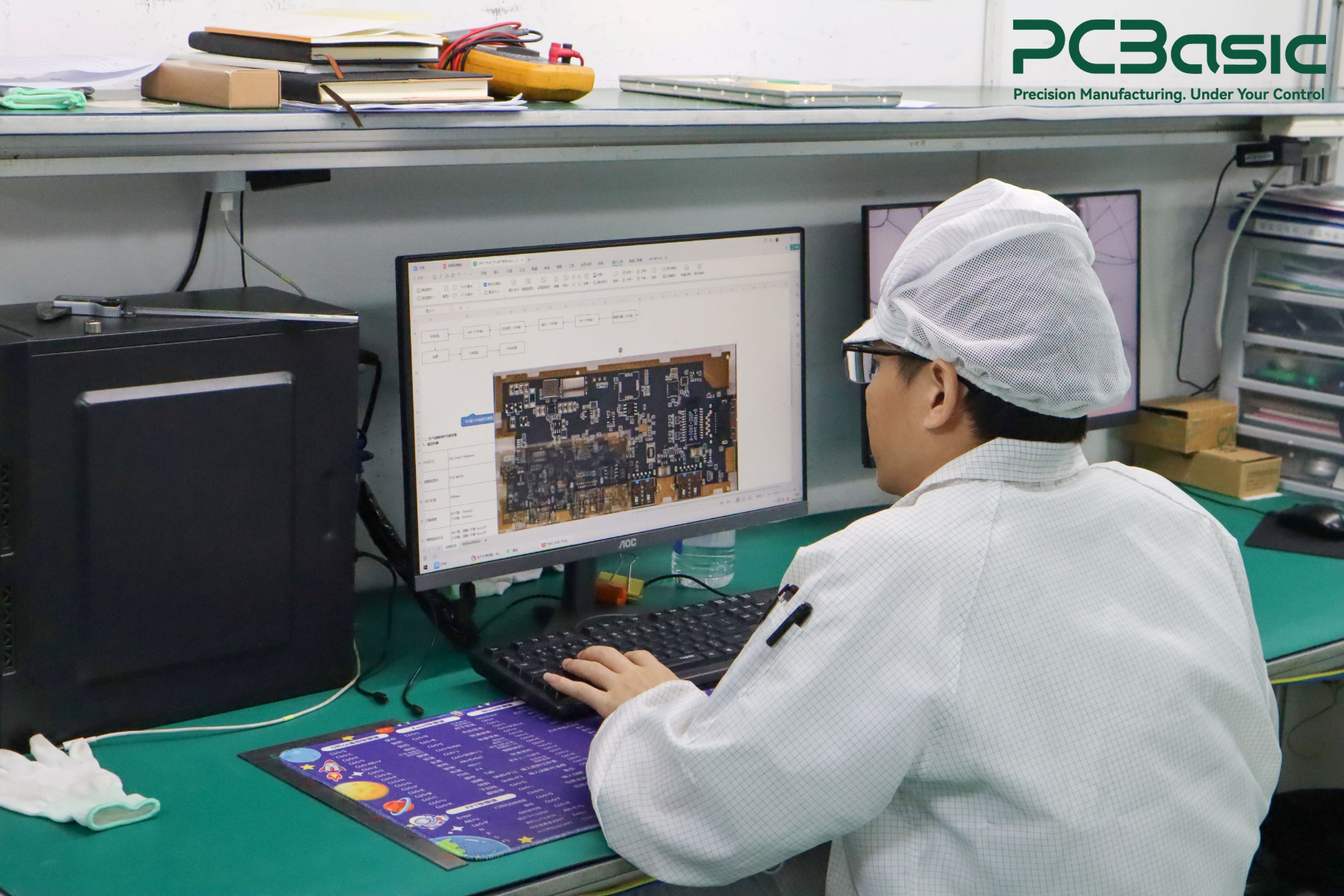
The engineering department makes sure that the PCB footprints match the BOM part numbers, as well as if the polarity markings coincide with silkscreen and also that there are enough rails in the array for the SMT line. Even neglecting it when doing telecommunications PCB assembly will make more work than it actually saves.
The good telecom PCB assembly services view the BOM review as dialogue and not as a barrier. Engineers warn about panel utilization, tooling holes and test points accessibility from the very beginning to be able to correct the layout design without any additional expenses.
There is inherent risk associated with BOM review as well. Long lead-time RF components, allocation restricted connectors and parts approaching end-of-life status can hold up the production for months; therefore, engineers warn about possible issues and offer form, fit and function substitutes for such items.
DFM validation points out problems that will be found during the assembly process, like incorrect solder mask dams that exist between pads connected directly to large copper areas without suitable thermal relief, which can cause uneven heating and soldering difficulties, or unfilled or improperly capped via-in-pad structures that allow solder to wick into the vias, reducing solder volume or contributing to voiding. Spotting these mistakes at this stage means that the timeline of the telecom PCB assembly process can be kept in line.
Traceability also begins during this stage. Lot codes, date codes, and component records that go back to a specific reel are of utmost importance in making telecom PCB assemblies than in other types of consumer assembly, since field failures require quick determination of the problem.
Planning for stack up affects almost all processes in production of telecom PCBs. If a layer stack is poorly planned in the beginning, later stages of the process will be significantly affected in terms of achieving signal integrity. Thus, engineers try to have a reference layer close to the signal layers, keep the thickness of dielectric materials consistent for controlled-impedance traces, and sometimes dedicate a separate grounding plane for the RF part of the circuit.
In 5G PCB assembly projects, the work becomes increasingly difficult, as some 5G hardware includes sub-6 GHz or mmWave RF sections, while other boards handle baseband processing, control, power, or data interfaces. Therefore, such aspects of design as routing of traces, the length of via stubs, and roughness of copper start to affect signal loss in a way that was unknown for much simpler designs.
Good planning of the stack up does not only allow producing PCBs with physical properties but also helps to make PCB manufacturing more reliable.
The placing of the components will influence power management as well as EMI performance. Power components require short and wide traces to provide current, while RF and clock circuits are isolated from fast switching areas to avoid electrical noise.
As far as the design of PCBA for wireless communications is concerned, it is better to separate the digital, analog, and RF sections to ensure board performance. In addition, the designer may include ground vias around shield can outlines.
RF shield cans can be used to isolate the sensitive receiver circuits from any nearby digital noise. It is also more efficient to decide on vent positions and gasket contact areas at the stage of PCB layout rather than PCB assembly.
When it comes to SMT assembly on boards sporting both fine-pitch BGA chips and RF shields, as well as press-fit connectors all on a single panel, you must think carefully about stencil design and reflow profiling.
In addition to that, mixed assembly that incorporates SMT and through-hole connectors may involve a second reflow cycle for double-sided SMT and selective soldering for the through-hole components later, which can damage parts already installed if not handled carefully.
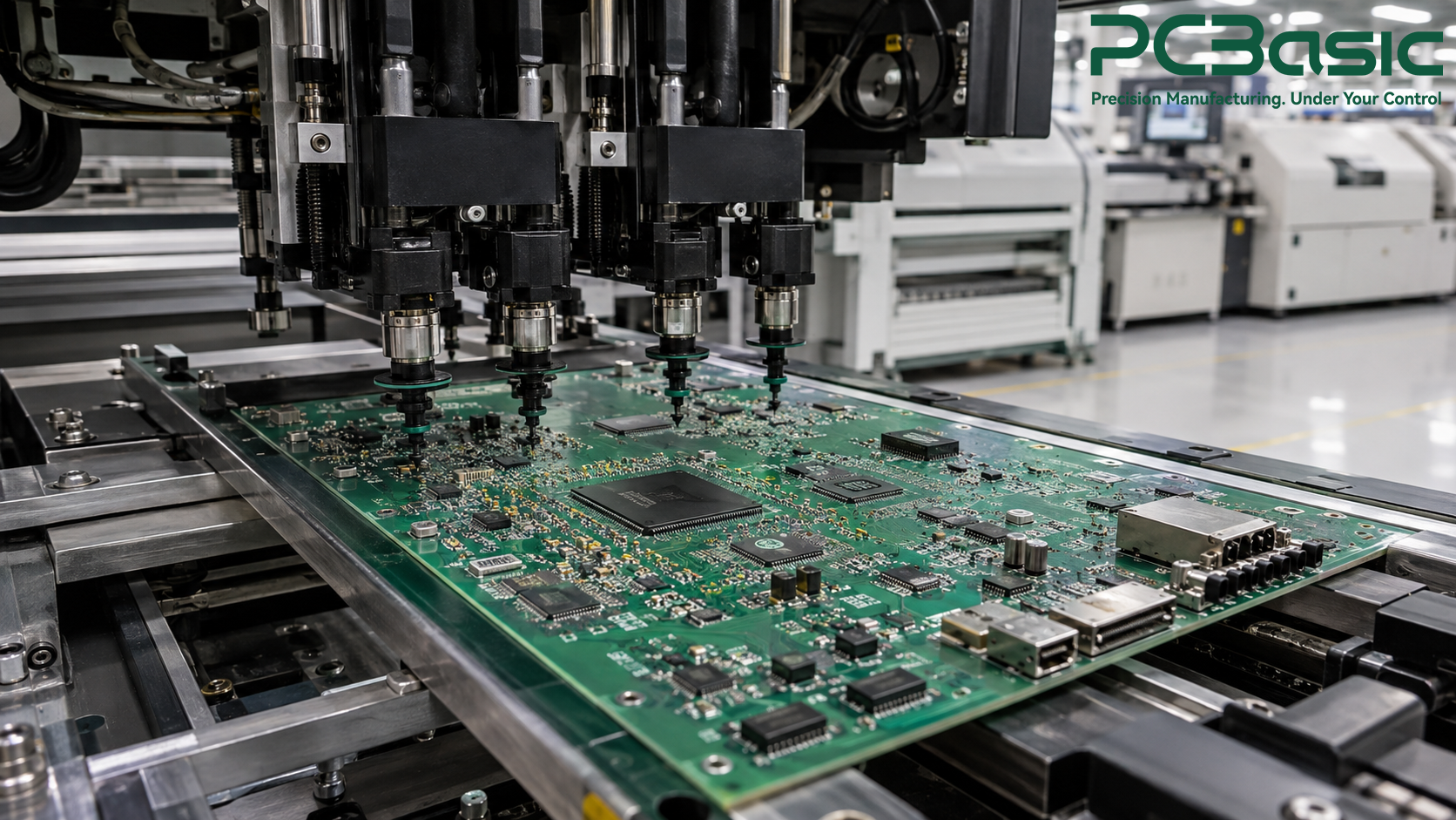
The inspection method should correspond to the level of risks of defects that the board presents and not follow a standard checklist. Engineers use automated optical inspection (AOI) for standard packages, while they use X-ray inspection for BGAs and QFNs because the solder joints remain hidden beneath the components.
Telecom PCB testing typically involves a combination of different methods. In-circuit testing uses a dedicated fixture and test program to check accessible nets for opens, shorts, and selected component values. Flying probe testing can perform many open, short, and component-level checks without a dedicated bed-of-nails fixture, making it suitable for prototypes and lower-volume production.
PCBA functional testing verifies whether the board is performing its intended function, testing the RF chains for proper function, detecting the data throughput, and ensuring the communication between a module and the network. Telecom PCB assembly and test programs extensively use unique functional fixtures at this stage, as the general "bed of nails" type of equipment is ineffective during RF path testing.
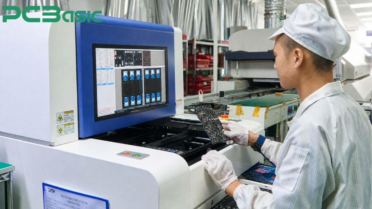
Environmental qualification or sample-based reliability testing may be required for boards intended for outdoor or thermally demanding environments. Short burn-in tests and thermal cycling are done to find out doubtful solder joints and bad components that pass room temperature functional test but fail during temperature changes.
The volume changes the equation. For a low-volume telecom PCB assembly project, flexible testing such as flying probe and manual functional test is best, since it may not be cost-effective to create a dedicated fixture for only ten assemblies.
For a high-volume telecom PCB assembly program, manufacturers use bed-of-nails fixtures and automated functional testers because they pay for themselves after processing a sufficiently large number of assemblies. It is important to plan for low- and high-volume telecom PCB assembly from the start of the program.
Choosing the right telecom PCB assembly supplier depends on assessing the engineering expertise of the vendor, not just price. This is due to the need to have experience in making controlled impedance boards, IPC-A-610 Class 3 assembly, RF shield, and conformal coating, which is typical for telecom products.
An experienced provider of telecom PCB assembly will be able to see potential risks in your design early on and offer feasible recommendations. When evaluating a supplier, check whether the manufacturer has experience with comparable high-speed, RF, outdoor, or long-lifecycle products and how it develops inspection and testing plans for such projects.
A full RFQ will minimize the possibility of delays and inaccuracies in quotation. It should contain Gerber files, BOM with part numbers of the manufacturer, assembly drawing, stack-up/impedance data, and testing criteria, e.g. flying probe or functional tests. And don’t forget about specifying the quantity for production so that the manufacturer could prepare tooling and test fixtures.
PCBasic applies such an engineering-based approach through the review of design files, early identification of any DFM problems, and provision of support from the prototype build to large scale manufacturing. This ensures that there is minimal risk during manufacture and increased product reliability.

Telecom PCB assembly, or telecom PCBA, makes or breaks itself well before the first board enters the reflow oven. Engineering, correct stack-up, DFM analysis, and a good test plan all go into ensuring reliable networks in the long term.
Designing with the assistance of a competent PCB assembly house during the initial stages allows companies to spot any potential problems before production even starts. By taking advantage of these techniques and using a competent PCB assembly company like PCBasic, companies will be able to transition from prototypes to manufacturing with ease.
Q1: What makes telecom PCB assembly different from consumer PCB assembly?
A1: Telecom PCB assembly aims at having a lifespan of about ten to fifteen years, higher control over the impedance, and an extended temperature range compared with many consumer boards, because service interruptions and field failures can have greater operational consequences.
Q2: How long does telecom PCB assembly take from prototype to production?
A2: Timelines depend on the board’s complexity, but a regular process takes from four to eight weeks from engineering reviews to prototype testing and further goes into volume manufacturing when the board passes the functional and environmental test phase.
Q3: What certifications should a telecom PCB assembly manufacturer hold?
A3: Look for ISO 9001 minimum standards, IPC-A-610 Class 3 build requirements if you need increased reliability, and ISO 13485 or AS9100 if your telecom infrastructure is medical- or aerospace-related.
Q4: Can one manufacturer handle both low-volume and high-volume telecom PCB assembly?
A4: Yes. There are many telecom PCB assembly services that have flexible SMT lines capable of supporting flying-probe-qualified prototypes that can easily scale to fixture-based manufacturing in large volumes without having to redesign at another facility.
Q5: What files does a telecom PCB assembly RFQ need?
A5: An RFQ should be a complete one that will include Gerbers, BOM with manufacturer part numbers, assembly drawings, fabrication notes with stack-up and impedance requirements, and test coverage for the board.
Q6: Why does material selection matter for telecom PCB assembly?
A6: It is important that low loss laminates maintain signal integrity at 5G and backhaul frequencies, while the choice of materials determines how well the circuit board will survive through many years of temperature cycling inside an outdoor enclosure, so it should be considered during design.

Assembly Enquiry
Instant Quote



Phone contact

+86-755-27218592
In addition, we've prepared a Help Center. We recommend checking it before reaching out, as your question and its answer may already be clearly explained there.
Wechat Support

In addition, we've prepared a Help Center. We recommend checking it before reaching out, as your question and its answer may already be clearly explained there.
WhatsApp Support

In addition, we've prepared a Help Center. We recommend checking it before reaching out, as your question and its answer may already be clearly explained there.
