Table of Contents
1. Power and Control
Boards in a Solar Inverter
2. Why Power and Control
Boards Require Unique Assembly Strategies
3. Solar Inverter PCB
Assembly Process
4. How Solar Inverter
Power and Control Boards Are Tested
5. Scaling from a Working
Prototype to Volume Production of Solar Inverters
6. Conclusion
7. FAQs
Solar energy inverter
installations grew more than 20% globally in the last calendar year. This is
primarily attributed to falling hardware costs and clean energy targets. Most
grid-connected solar power systems have a very important part: the solar
inverter. Solar inverters use advanced electronics to convert and control electrical
power at relatively high currents. Designing and manufacturing a solar inverter
PCB assembly is a great way to learn about modern manufacturing.
The PCBs of inverters
present a unique challenge due to the combination of high power and low digital
control. We will walk you through our process to give you some insight into our
work on the factory floor.
You will learn how
control chips are treated differently, how power is routed, and why extensive testing
is important to the longevity of our devices. This article, available on our
PCBasic blog, can help the mechanical, hardware, and purchasing teams as they
prepare to embark on their manufacturing journey.
Power
and Control Boards in a Solar Inverter
Solar Inverter Power
PCB
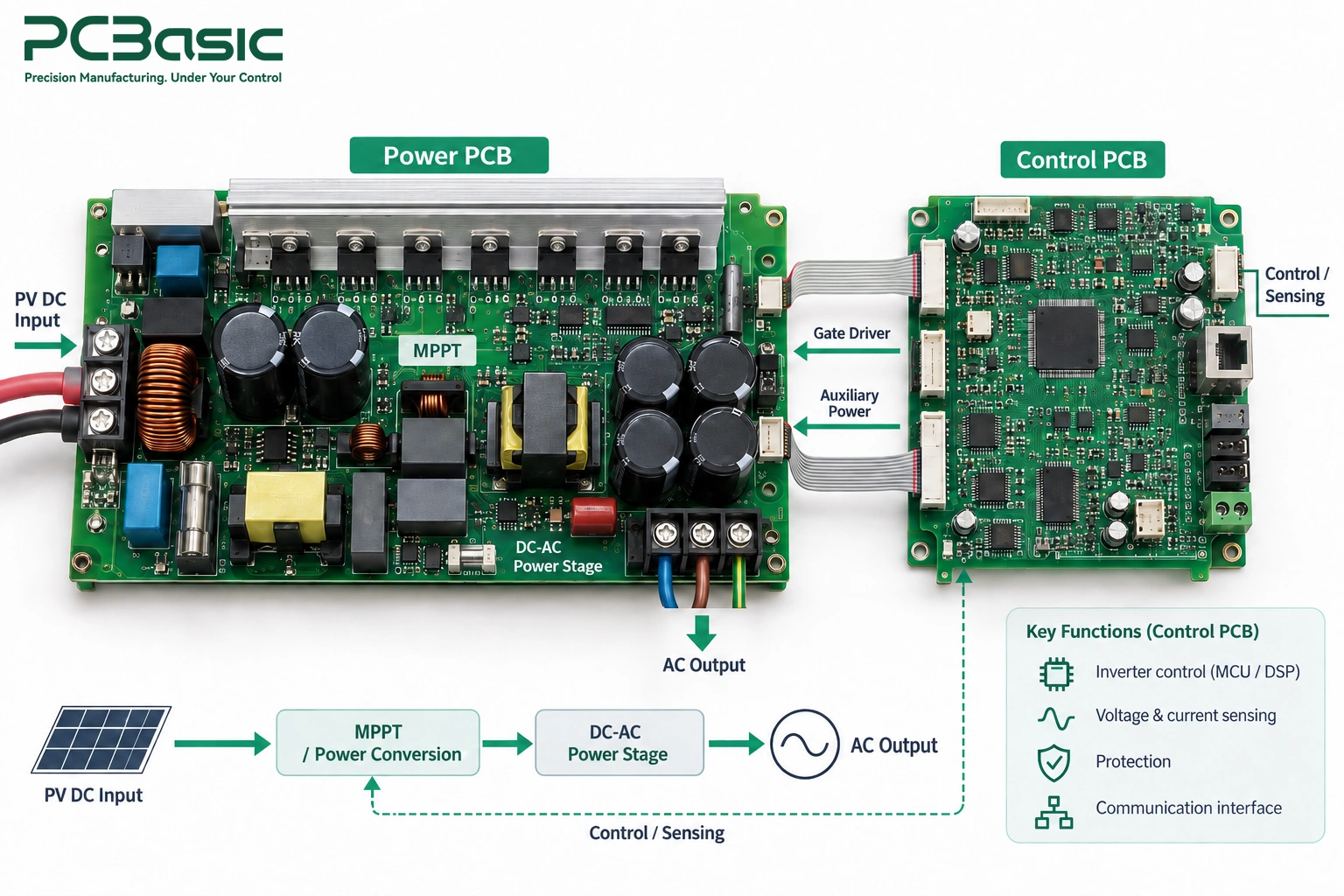
A solar inverter power
PCB contains specialized electronics in its power section that convert DC power
from solar panels into usable AC power. A solar inverter system relies heavily
on this power section, so it must have great resistance against heat.
Heavy copper traces act
like wide electrical highways, allowing higher currents to flow with lower
resistance and helping reduce excessive heat buildup. Fabricators may build
these boards using heavy copper layers, typically ranging from 2 oz to 4 oz or
more depending on the design. Large electrolytic capacitors and power switching
transistors (such as MOSFETs or IGBTs) are commonly used in a solar inverter
PCB assembly.
Solar Inverter Control
Board
The power section might
act like the system's muscle, but the solar inverter control board works like
the system's brain. This part of the system generally operates at much lower
voltages, often using low-voltage rails such as 3.3V, 5V, or other levels. This
part of the circuit includes microcontrollers and digital signal processors
(DSPs).
At much lower voltages,
the control board monitors system conditions in real time and responds to input
conditions. This board communicates with external monitoring systems and checks
thermal sensors and input voltages.
MPPT, Gate Driver,
and Auxiliary Circuits
Inside the control
system, other specialized circuits perform additional functions, improving
power conversion efficiency. One of the control system circuits is the MPPT,
and this circuit continuously evaluates the voltage at which the panels produce
peak output based on changing operating conditions.
Meanwhile, gate-driver
circuits work like very important translators on the solar inverter PCB. The
biggest reason is that low-voltage microcontroller pins cannot directly switch
high-power IGBTs, so gate drivers amplify and condition the control signals.
Alongside these drivers, auxiliary power circuits step down internal voltages
and provide stable power to the inverter control PCB even during normal
operation.
Why
Power and Control Boards Require Unique Assembly Strategies
Electrical and
Thermal Demands on the Power PCB
Manufacturing a solar
inverter power PCB comes with unique challenges that most consumer electronic
products do not. Large copper planes dissipate heat, but they also draw heat away
from the soldering joint during the PCB
assembly process.
The high mass of such a
PCB also causes issues with reflow ovens, as heating profiles that work for many
standard PCBs do not work well for power PCBs. It may take highly customized
factory oven profiles to produce PCBs for a solar inverter if the technicians
working on it are to avoid cold joints.

Fine-Pitch and
Sensitive Circuits on the Control PCB
The world of precision
on a solar inverter control board is very different from what we saw on the
power board. This board may employ microchips with fine pin spacing, including
QFN, BGA, and other packages with pitches below 0.5 mm.
These packages can be
damaged when exposed to temperatures beyond their specified reflow limits.
Squeegee pressure and solder paste printing parameters for this process also have
to be very controlled, as excess solder paste can easily connect to adjacent
pads and ruin the solar inverter PCB assembly process.
Mixed Component Sizes Create Process Challenges
When a design combines a
power section and a control PCBA section, working with a standard solar
inverter PCBA process becomes challenging.
Advanced processes may use
stepped stencils or optimized stencil apertures to alleviate this issue. Highly
precise metal sheets deposit a thick paste where large components reside and a
thin paste where fine-pitch microchips are. Deciding on a PCB assembly strategy
early on helps avoid time-consuming and costly reworks later.
Solar
Inverter PCB Assembly Process
DFM, BOM, and
Assembly Review
An engineering audit
before any assembly machines run is an important part of every production
manufacturing process. During the Design for Manufacturing (DFM) audit, pad
geometries, component spacing, and thermal relief are reviewed in detail in the
bare board files. The team also reviews the Bill of Materials (BOM) and
verifies that high-power transistors and special control chips match the
approved part numbers and sourcing requirements. This step helps avoid
time-consuming and costly delays in the solar inverter PCB assembly process.
SMT Assembly
With engineering
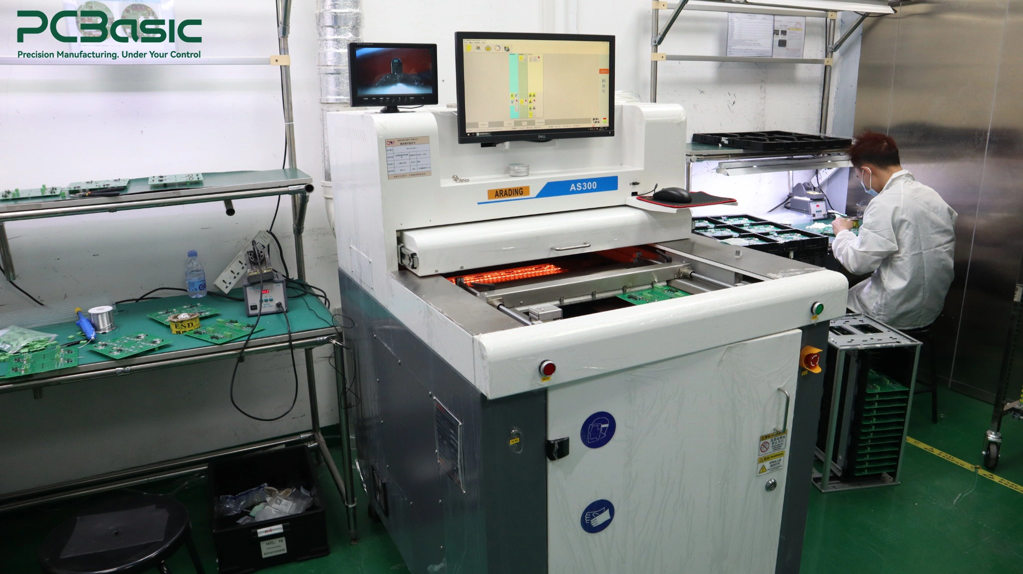
clearance, Surface Mount Technology (SMT) begins. Automated printers precisely
deposit solder paste onto the copper pads using laser-cut stencils. SPI systems
confirm paste height, volume, and coverage.
Precision-placing
surface-mount parts occurs next. The solar inverter PCB then goes through a multi-zone
reflow oven. Every component is soldered in place through
temperature-controlled reflow of the deposited solder paste.
Through-Hole and
Odd-Form Assembly
Large and heavy
components such as transformers, large capacitors, and terminal blocks often
use through-hole
PCB assembly for additional mechanical support. Heavy components may not be
able to rely only on surface solder pads for mechanical support.
Technicians or robots
place part leads into plated board holes and insert them. Then the assembly
enters a selective or wave soldering system. Selective soldering protects
sensitive portions of the PCB from excessive heat by directing liquid solder
only to specific pins.
Cleaning, Coating,
and Mechanical Assembly
After soldering, the
board may need to be cleaned to remove chemical flux residue, depending on the
flux chemistry and cleanliness requirements. Automated inline washers may use
deionized water or other qualified cleaning processes to scrub the board and to
prevent stray electrical leakage.
The solar inverter may also
require additional environmental protection, as it may be exposed to harsh
conditions on rooftops or in basements. A conformal coating process may apply a
thin acrylic or silicone film to the PCBA, forming a protective layer against
moisture, dust, and other airborne pollutants.
How
Solar Inverter Power and Control Boards Are Tested
SPI, AOI, and X-Ray
Inspection
Quality control starts
long before final power-up. Solder paste inspection (SPI) is performed to
verify the paste volume after printing. If the paste volume drops below the
acceptable level, the board is held for review before components are installed.
After reflow soldering,
component alignment, polarity, and joint geometry are checked by automated
optical inspection (AOI) systems. In addition, 3D X-Ray inspection (AXI)
systems can inspect power transistors with hidden belly pads, as well as power
PCBs for voids in the solder on thermal pads.
ICT, Flying Probe,
and Electrical Checks
Once the boards have
passed visual inspections, a variety of electrical tests are done to check the
integrity of the assembly. In-Circuit Testing (ICT) uses bed-of-nails fixtures
and can measure thousands of test points for resistance and capacitance and
verify continuity.
For smaller batches and
prototypes, flying probe testers employ robotic arms for touch testing. This is
much more cost-effective than fabricating tooling to test accessible points for
short circuits and open connections on solar inverter PCBAs.
Testing the Control
Board
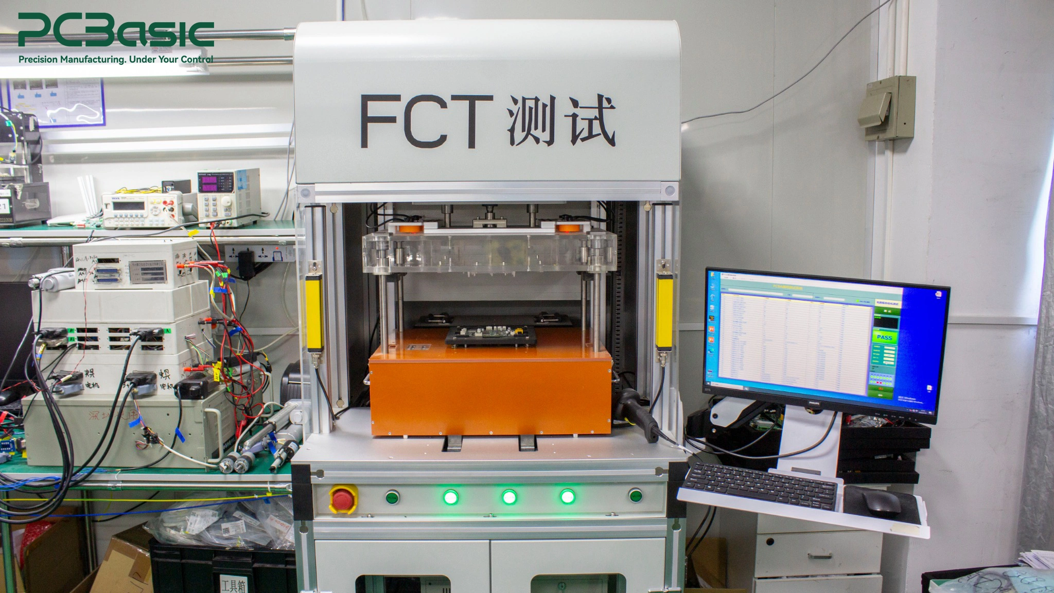
Depending on the test
plan, the solar inverter's control board then undergoes firmware loading and
functional testing. The board may be mounted on an automated test fixture that
simulates defined solar panel input and grid-related signals.
The test routine may also
exercise the code, verifying the communication ports (CAN, RS485, or Wi-Fi),
and verifying sensor measurements or calibration where required. Ensuring the
control PCB of the solar inverter processes telemetry correctly helps verify that
the inverter responds as intended to real-world grid variations.
Validating the Power
Section
Functional testing of
the power section requires additional complex test setups. Electrical and
thermal loads may be applied to the solar inverter power section during
validation using controlled DC input conditions. Real-time thermal
probes or thermal imaging may be employed to assess the distribution of
environmental temperature and the yield of heavy copper traces.
Scaling
from a Working Prototype to Volume Production of Solar Inverters
Validating Prototype
and Pilot Builds
Transforming a concept
of solar inverters from CAD to practical market distribution requires a careful
series of steps. The initial prototype builds (usually 5-20 units) verify the
hardware and the mechanical fit in the inverter enclosure.
Once a prototype is
approved, a small pilot production run (50-200 units) is made to test high-volume
production. Engineers are then able to scale up production by fine-tuning
pick-and-place motions, tool stencil designs, and soldering. Fixing and
refining minor assembly issues during pilot manufacturing helps reduce issues
during subsequent mass production.
Production Control
and Traceability
Higher reliability in
electronics requires total visibility in manufacturing. Many factories apply a
unique 2D matrix barcode or serial number to each board before manufacturing.
Each workstation along
the manufacturing line features a barcode scanner. Scanning each barcode can
link the board to a component’s lot number, process records, and the results of
the test. In the event of a failure many years later in the field, this
traceability data aids an inverter PCB manufacturer in more rapidly investigating
the root cause.

What to Provide a
Solar Inverter PCB Manufacturer
A complete documentation
package should be provided to receive a production quote without engineering
delays. Your provided package should include Gerber or ODB++ layout files, a
complete Bill of Materials with manufacturer part numbers, pick-and-place coordinate
files, and assembly drawings.
Clarify the copper
weight, PCB material, and solder mask requirements, and specify the required IPC
workmanship or acceptance standards (such as IPC-A-610 Class 2 or Class 3) and
the required conformal coating. This clarity allows your solar inverter PCB
manufacturer to set up their line with fewer engineering clarification cycles.
PCBasic's
Capabilities
PCBasic has extensive experience in
assembly for power requirements in solar inverter PCB manufacturing and offers
quick-turn prototyping and high-volume production.
Generally, we
incorporate advanced SMT technology, along with 3D SPI and AOI systems, and have
dedicated soldering and burn-in test systems. From heavy-copper solar inverter
power PCBs to dense, multi-layer inverter control PCBs, our engineering team is
here to offer comprehensive support to ensure your product performs well in the
field.
Conclusion
There is a need to
integrate high-power distribution with the digital control of microchips.
Successful assembly of a solar inverter PCB requires carefully DFM review, SMT
and through-hole soldering, and multiple extensive tests. By understanding the
factory processes, engineering teams can develop better products and choose
manufacturing partners with a focus on long-term reliability.
FAQs
Q1: What copper thickness is
required for a solar inverter power PCB?
Many high-current power
boards may use 2-4 oz copper layers or more, depending on current and thermal
requirements.
Q2: Why are power and control
boards often separated in solar inverters?
Placing power boards
away from the control boards helps protect sensitive control circuitry from
thermal buildup and electrical noise generated by the power section.
Q3: What is the benefit of
conformal coating on a solar inverter PCBA?
Conformal coating helps
protect the PCBA from dust, moisture, and corrosive environmental contaminants.
Q4: How does 3D X-Ray testing
improve solar inverter PCB quality?
3D X-Ray inspection of
solar inverter PCBs can detect hidden voids beneath bottom-terminated power
devices and thermal pads that affect PCB thermal transfer.