Table of Contents
1. What Is an Edge AI Module PCBA?
2.
Why Edge AI Module PCBAs Are Difficult to Manufacture
3.
From PCB to Assembled Edge AI Module
4.
Testing an Edge AI Module Before Integration
5.
Conclusion
6. FAQs
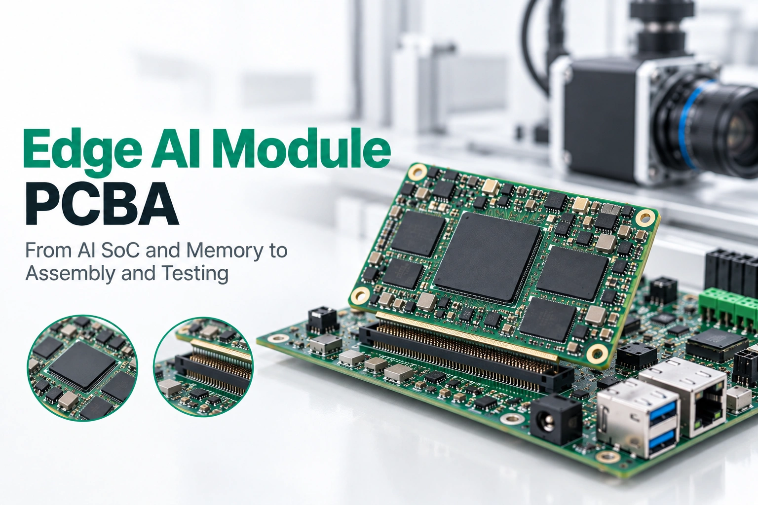
An edge AI module
PCBA may not seem large in size, but it often integrates AI SoC or NPU,
high-speed memory, Flash, power management, clock circuits, as well as PCIe,
MIPI, USB and other high-speed interfaces. To enable the device to perform AI
inference locally, these key components need to be concentrated within a
limited PCB area.
This also
means that edge AI module PCB assembly is more complex than ordinary embedded
control boards. AI processors and high-speed memory are usually packaged using
high-density methods such as BGA, with solder joints hidden at the bottom of
the components. Visual inspection alone cannot confirm the soldering quality.
At the same time, high-speed signal integrity, power stability and thermal
management are also key aspects to focus on in the manufacturing of such
modules. Any control failure in any of these aspects can affect the module's
startup, communication or long-term operation.
Therefore,
whether an AI module PCBA can smoothly progress from a prototype to mass
production cannot only be determined by whether the components are properly
mounted, but also by paying attention to issues such as solder paste printing,
BGA soldering, X-Ray inspection, functional testing and the connection between
the module and the carrier board. This article will start from the hardware
composition of the module and further analyze key problems in high-density
assembly, BGA soldering and testing.
What Is
an Edge AI Module PCBA?
Edge AI module
PCBA is a small-sized assembly circuit board that mainly performs AI
computations at the device level. It is not typically a complete system
motherboard but rather integrates the core components such as the processor,
memory, storage, power management, and high-speed interfaces onto a compact
module.
A typical
edge AI module PCB usually includes:
• AI SoC, NPU, GPU or dedicated AI accelerator
• LPDDR memory
• eMMC or Flash storage
• PMIC and related power circuits
• Clock components
• High-speed interfaces such as PCIe, MIPI, USB, etc.
• Board-to-board connections or connection interfaces between the
module and the carrier board
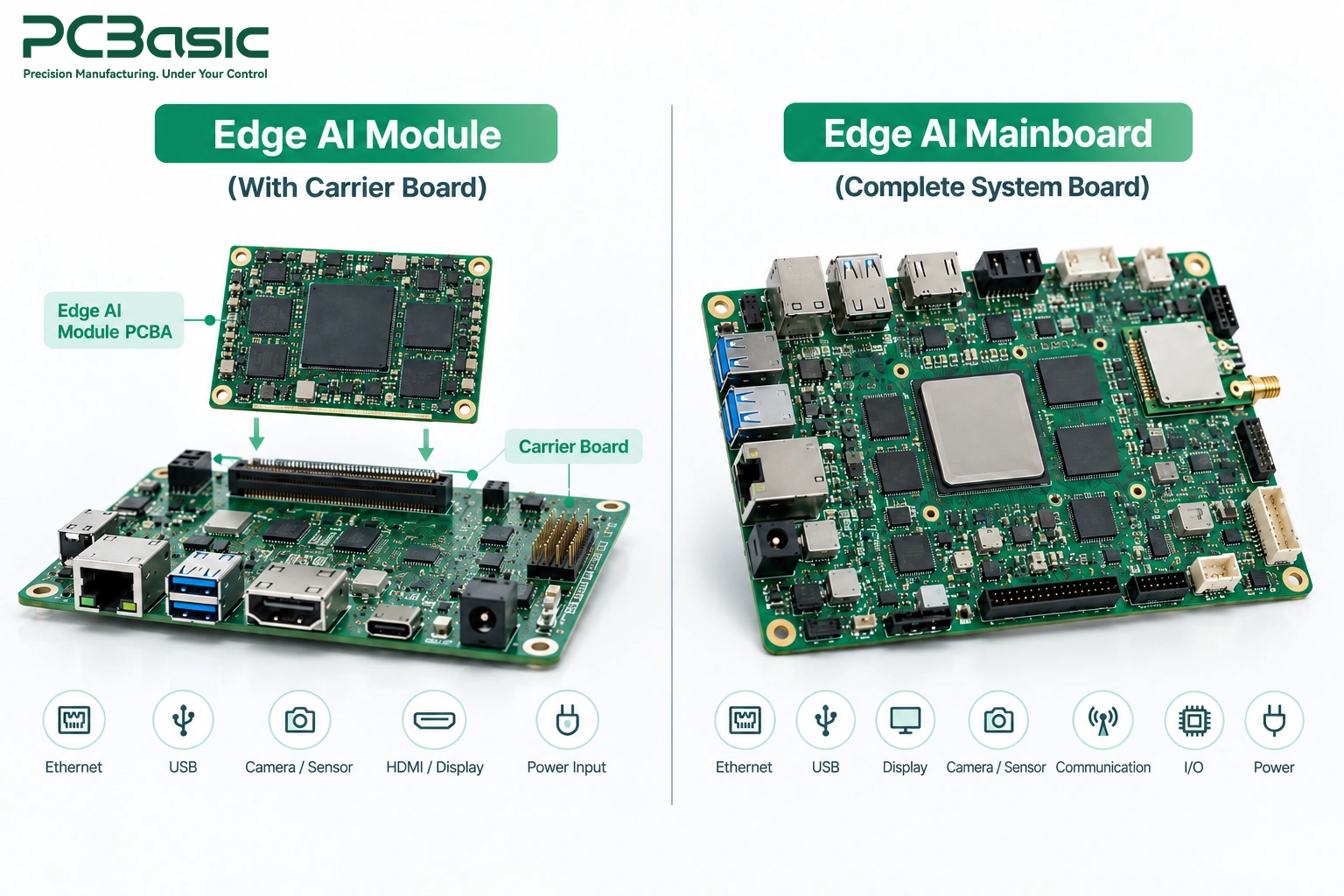
If the main function of a module is to provide AI processors, memory,
storage and power support, then it can also be regarded as an edge AI computing
module. Such modules usually do not complete all the product functions
independently, but are connected to the carrier board for use. The carrier
board is responsible for I/O, communication, sensors and other interfaces
related to specific products.
The difference between the edge AI module and
the complete edge AI motherboard can be simply understood as follows:
|
Item
|
Edge AI Module
|
Complete Edge AI
Motherboard
|
|
Main function
|
Provides core AI computing capability
|
Completes the functional integration of the
entire system
|
|
Main hardware
|
AI processor, memory, storage, PMIC,
high-speed interface
|
AI computing part, as well as communication,
I/O, sensors and main power input
|
|
Usage method
|
Usually connected to the carrier board or host
system
|
Usually used directly as the main system board
|
|
Design focus
|
Compact size, high computing density, easy
reusability
|
Complete functionality and system integration
|
The advantage
of this modular design is that the same AI computing platform can be more
conveniently applied to different products. However, at the same time, more
critical circuits are concentrated within a limited PCB area, which also
imposes higher requirements on the precision, stability, and production
consistency of AI module PCB assembly.
Why
Edge AI Module PCBAs Are Difficult to Manufacture
The main
challenge of edge AI module PCB assembly is to integrate the processor, memory,
power circuit and high-speed interface within the limited PCB area. As the
distance between components becomes shorter, the requirements for assembly
accuracy and manufacturing consistency will also increase.
High-Density Components and BGA Soldering
AI SoC, NPU
and memory usually adopt BGA or other fine-pitch packaging, and small passive
components are also distributed around them. In high-density PCB assembly, solder
paste printing, component placement and reflow require more stringent control.
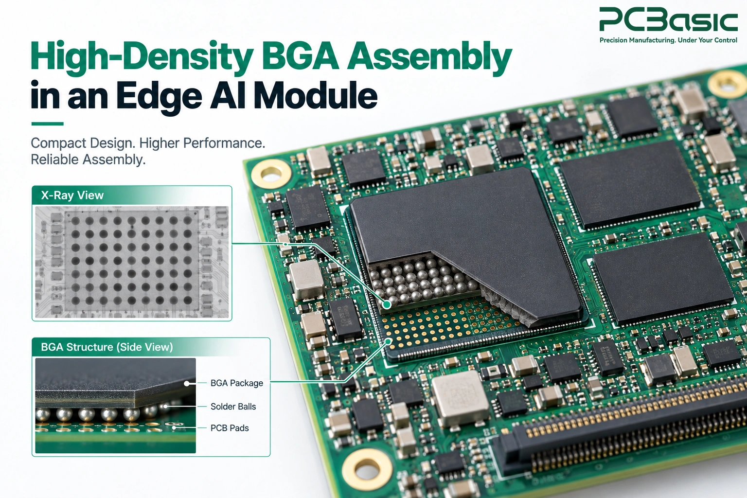
For fine-pitch BGA assembly, since the solder
joints are hidden at the bottom of the components, AOI or visual inspection
cannot conduct a complete check, so X-Ray inspection may also be needed.
High-Speed Signals and PCB Routing
LPDDR memory
as well as interfaces such as PCIe, MIPI, and USB are highly sensitive to
manufacturing deviations. The PCB can adopt impedance control, HDI structure,
microvias, or via-in-pad to meet the requirements of high-density routing and
BGA fan-out based on the design.
Power Supply and Heat Dissipation
The AI
workload can result in rapid change of the power consumption demand of the
processor. Meanwhile, the processor and memory will produce heat in a
relatively small area. Thus, considering both stable power supply and effective
thermal paths simultaneously is needed in the PCB layout and construction.
Inspection and Testing
Some problems
are noticed only after the module is powered on. Depending on the
circumstances, you may need to do X-Ray inspection, programming, functional
testing or interface testing to find hidden BGA soldering defects, unstable
power rails or interface problems.
Hence, AI hardware PCB assembly is not a
mere component mounting job. The stable and consistent mass production of the edge
AI module depends on PCB fabrication, assembly, inspection, and testing.

From
PCB to Assembled Edge AI Module
The
bare board can be assembled into a full AI module PCBA following PCB design and
BOM confirmation. The steps are as follows:
• Solder
paste printing and SPI: In order to detect printing
problems prior to component placement, solder paste is first printed on the PCB
pads and then its volume, location, and form are checked using SPI.
• SMT assembly and reflow: After being
constructed using SMT equipment, AI processors, memory, PMICs, and passive
components go through the reflow soldering process. Stable printing,
positioning, and reflow procedures for AI module PCB assembly help minimize
variations in quality between batches.
• AOI and
X-Ray: AOI inspection comes first after reflow
soldering. X-rays can be utilized for further confirmation for solder joints
(like BGA) that cannot be directly seen.
• Testing and
traceability: Following assembly, firmware programming
and functional testing can be done in accordance with the module requirements.
Revisions to the PCB and BOM, materials, inspection records, software, and test
results can all be tracked for repeat manufacture.
For edge AI module
PCBA, PCBasic will select the appropriate inspection and testing methods based
on the specific board design and customer requirements, including SPI, AOI,
X-Ray and PCBA functional testing, and will
also trace the production process. These steps not only help confirm whether
the prototype is normal, but also help maintain stable assembly quality after
the project enters repeated production.
Testing
an Edge AI Module Before Integration
Passing
assembly inspection does not mean that the edge AI module PCBA installed in the
final product will definitely work properly. Before the formal integration, we
still need to power on the module to see if it can start and run normally.
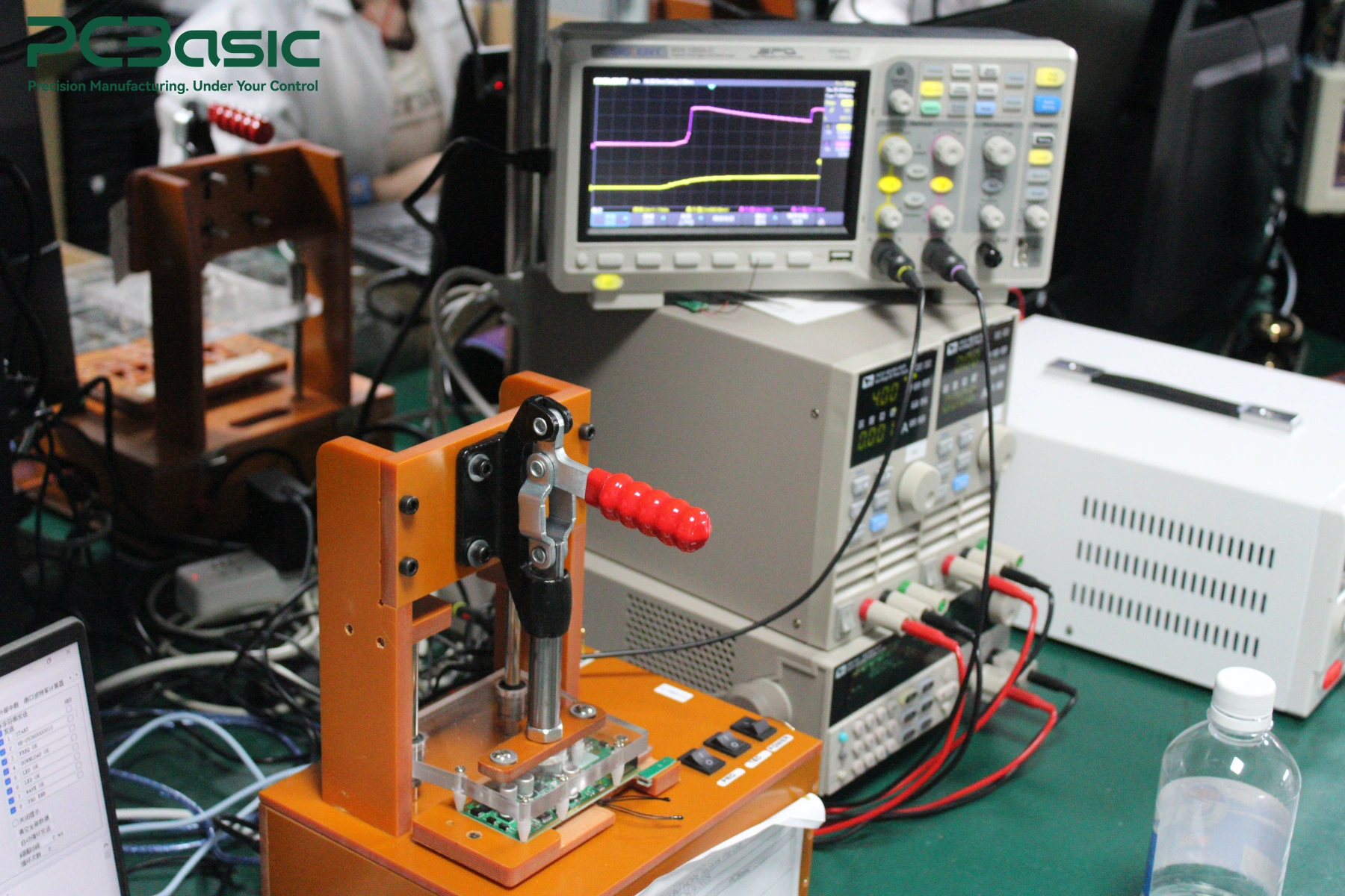
First, we can
check the power rails, current, and startup status. If these are all normal,
then we can program the firmware or system image according to the module design
and check the memory, storage, and key interfaces such as PCIe, USB, Ethernet,
and MIPI. After that, we can also conduct functional testing to confirm whether
the main functions of the AI module PCBA are normal.
The performance after the module is connected to
the carrier board also needs to be paid attention to. Some modules may not have
problems when tested alone, but after being connected to the carrier board,
they may show problems due to power supply, connectors, communication
interfaces, firmware settings, or thermal contact. Therefore, the testing of AI
module PCB assembly cannot only focus on the module itself, but also consider
how it will be connected and used in the final product.
If the module
needs to run for a long time or handle a high AI workload continuously,
additional thermal testing, aging testing, or load testing can be conducted
according to project requirements. What to test, test for how long, and what
results are considered acceptable should all be determined based on the actual
product and customer requirements, rather than applying a fixed set of Edge AI
testing standards.
Conclusion
For the edge
AI module PCBA, creating a working prototype is not the end goal. Once it
enters production, what's more important is whether the same design and process
can be used to consistently produce modules with stable quality.
Therefore,
when developing the edge AI compute module, it is best to consider
manufacturing issues from the early stage of the project rather than addressing
them one by one after the prototype is completed. The better the coordination
among design, materials, assembly, and testing, the smoother the transition
from the prototype to volume production will be.

If you are
developing an edge AI module PCBA, PCBasic can provide one-stop manufacturing support including PCB manufacturing,
component sourcing, AI module PCB assembly, X-Ray inspection, programming,
functional testing, and production traceability. You can send us your Gerber
files, BOM, and project requirements, and we can further communicate your manufacturing
needs for the Edge AI module.
FAQs
Q1: What
is the difference between an Edge AI module and an Edge AI mainboard?
An edge AI
compute module mainly contains the processor, memory, storage, and power
circuits and usually connects to a carrier board. A mainboard integrates these
functions with more product-specific I/O and interfaces on one PCB.
Q2: Why is
BGA assembly important for Edge AI modules?
AI processors
and high-speed memory often use BGA packages to save PCB space. Fine-pitch BGA
assembly requires accurate printing, placement, reflow, and inspection because
the solder joints are hidden beneath the package.
Q3: Does
every Edge AI Module PCBA require HDI?
No. It
depends on component density, package pitch, routing, and interface
requirements. Some compact modules may use HDI, microvias, or via-in-pad to
support dense routing.
Q4: How is
an Edge AI Module PCBA tested?
Testing may
include power-on checks, programming, memory and interface checks, and
functional testing. Thermal, aging, or module-to-carrier testing can also be
added when required.