
Global high-mix volume high-speed PCBA manufacturer
9:00 -18:00, Mon. - Fri. (GMT+8)
9:00 -12:00, Sat. (GMT+8)
(Except Chinese public holidays)





HomePage > Blog > Knowledge Base > IoT Module PCB Assembly Service: Manufacturing, Testing, and Reliability
1. What Is IoT Module PCB Assembly?
2. Key Manufacturing Challenges in IoT Module PCB Assembly
3. IoT Module PCB Assembly Process: From BOM to Finished PCBA
4. Testing and Quality Control for IoT PCB Assemblies
5. Choosing an IoT PCBA Manufacturer: From Prototype to Production
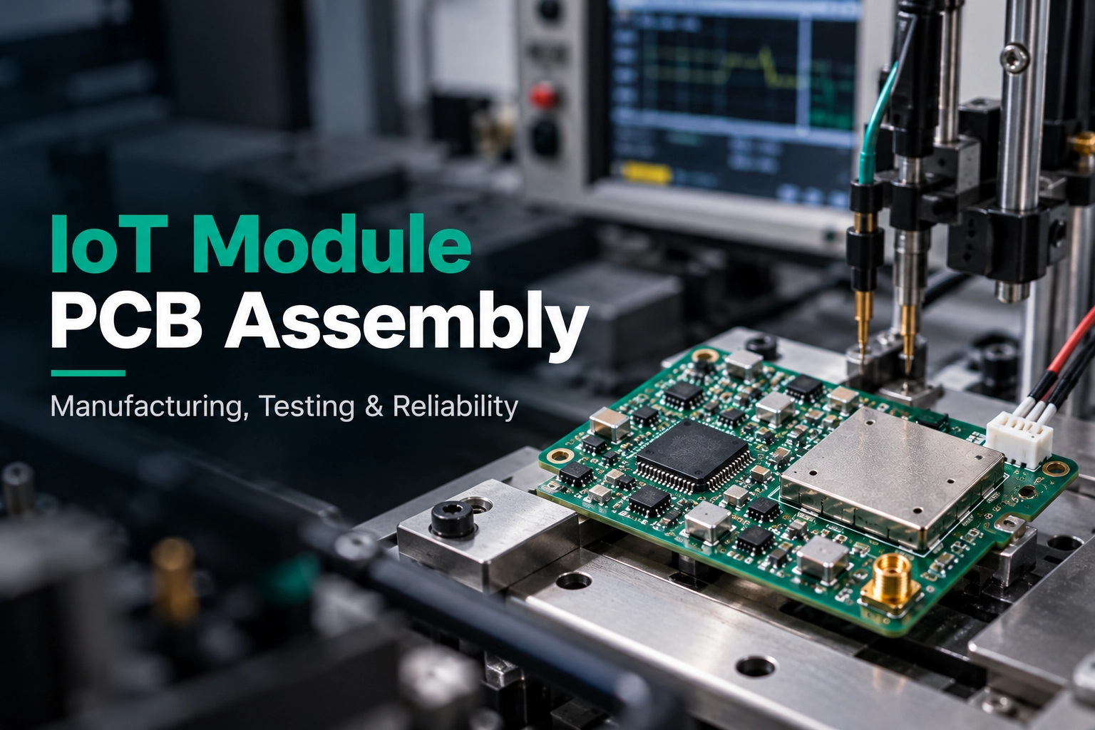
So, how can IoT modules smoothly move from the prototype stage to mass production? Good design is just part of the answer. The manufacturing process is equally important. This article will focus on IoT PCB assembly services, introducing common assembly challenges of IoT modules, SMT production processes, quality inspection and functional testing, as well as several issues to consider when choosing a PCBA manufacturer.
The process of mounting and soldering electronic components onto printed circuit boards used for networked devices is known as IoT module PCB assembly. IoT modules typically integrate several functionalities in a constrained area, in contrast with basic circuit boards with a single purpose. Depending on the product, it could consist of:
• Microcontroller (MCUs): Data processing and device operation control.
• Wireless module: facilitates cellular, Bluetooth, Wi-Fi, and LoRa connectivity.
• Sensor and GPS/GNSS module: Gathering position or environmental data as needed.
• Power management circuit: controlling power usage and voltage.
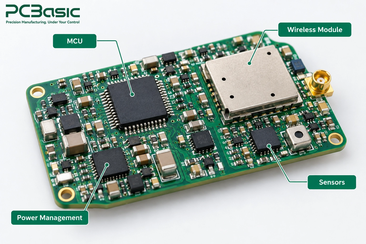
Component sourcing, SMT assembly, through-hole soldering if required, inspection, and functional testing are usually included in the IoT module PCB assembly service. Radio frequency shielding, enclosure assembly, and firmware programming may also be necessary for some projects.
IoT PCB assembly is used in smart meters, GPS trackers, industrial sensors, and smart home appliances. They don't necessarily have the same production needs, though. While industrial sensors might need more durable connections and protection from hostile environments, battery-powered GPS trackers need minimal power consumption and a reliable wireless connection. Before production starts, these distinctions should be considered.
For IoT circuit boards using 0201 or 01005 components, as well as QFN and BGA packages, the process of mounting and soldering is not simple. Due to the small size of the components and the narrow spacing of the pads, even a slight increase or decrease in the amount of solder can affect the soldering quality. Some products may also use HDI or rigid-flex PCBs, which impose additional requirements on the positioning, support, and handling during the production process.
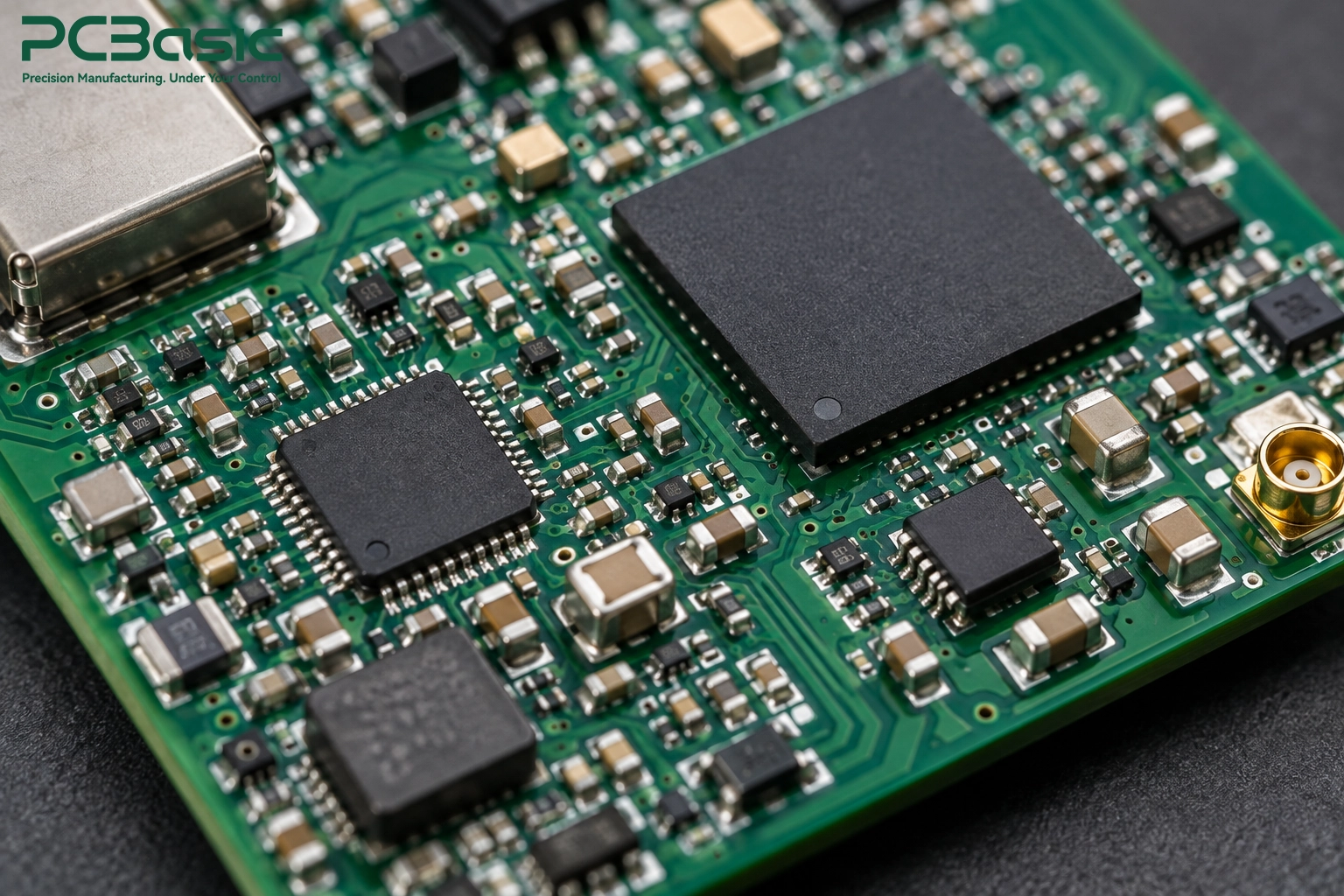
During the SMT assembly for IoT devices, we typically focus on the following issues:
• Insufficient solder paste: May lead to poor solder joint or open circuits.
• Component offset: May cause poor soldering, and in severe cases, even bridging.
• Inappropriate reflow profiles: May cause soldering defects, and even damage components sensitive to temperature.
How to control these issues? Manufacturers need to start from solder paste printing, placement accuracy, and reflow soldering processes, and conduct inspections at different stages. PCBasic supports precise SMT assembly for small components and fine pitch packaging. We also equip with SPI, AOI, and X-ray inspection equipment to help detect assembly defects during the production process.
Does the fact that the wireless module can be powered on mean that there are no communication issues? Not necessarily. Even if there are no obvious issues in the PCB design, poor solder joints, improper installation of RF connectors, or shielding defects may still affect wireless communication.
In wireless module PCB assembly, we need to check the installation of RF components, antenna connections, and shielding components according to the actual requirements of Wi-Fi, Bluetooth, LoRa, or cellular communication modules.
To prevent making modifications that do not match the design criteria throughout the assembly process, we must adhere to the confirmed antenna exclusion zones and component layout requirements for RF module PCB assembly. However, antenna design and impedance matching are design concerns that cannot be resolved by just improving soldering quality.
Wireless sensors and GPS trackers typically need to run for a long period, and some devices are difficult to dismantle for maintenance after installation. Therefore, during assembly, not only should the correctness of component soldering be checked, but also the stability of connections in actual use and environmental impacts should be considered.
For example, a GPS tracker may start up normally, but due to poor antenna connection, it is always unable to achieve stable positioning. For low-power IoT PCB assembly, manufacturers also need to check the soldering quality of power management components to avoid assembly defects that affect the normal operation of the circuit. As for whether the device can achieve the expected low power consumption, it also needs to be judged in combination with circuit design, firmware and actual test results.
If the product needs to operate in vibration, temperature changes or humid environments, manufacturers should also confirm the corresponding protection, assembly and testing requirements in advance, rather than waiting until problems appear after the product is put into use.

Before the IoT module enters production, we need to check not only the PCB design. The BOM, component supply situation, assembly instructions and test requirements must also be clear. If necessary information is lacking at this stage, it may lead to subsequent production delays or problems.
First, we will review Gerber files, BOM, pick-and-place data, and assembly drawings. This helps us identify issues such as mismatch between the package and the pad, unclear component orientation, or lack of assembly instructions before production begins.
The wireless communication project may also require antenna specifications, shielding requirements, and firmware files.
Component sourcing is an important part of turnkey IoT PCB assembly. Even if the alternative components have similar specifications, they may affect wireless communication performance or power consumption. Therefore, we will confirm with the customer and obtain approval before using alternative components.
When the bare PCBs and components are ready, the assembly process usually proceeds as follows:
|
Assembly Step |
What Happens |
|
Solder Paste Printing |
Apply solder paste onto the PCB pads. |
|
SPI Inspection |
Check the volume, height and position of the solder paste. |
|
SMT Placement |
Place ICs, wireless modules, sensors and other SMDs. |
|
Reflow Soldering |
Form solder joints through controlled heating. |
|
AOI Inspection |
Inspect the component placement and visible soldering defects. |
|
Through-Hole Assembly |
Install and solder through-hole components as needed. |
Throughout the entire production process, small components and those sensitive to humidity need to be handled with care. At PCBasic, our PCB assembly services include SMT, DIP, inspection and testing, enabling us to handle different assembly requirements within the same production process.
After the soldering process is completed, some IoT circuit boards still require additional inspection, cleaning, firmware programming, or functional testing.
According to the specific requirements of the project, we may also need to install cables, apply conformal coating, or assemble the PCBA into the enclosure.
PCBasic can coordinate components sourcing, PCB assembly, and the necessary final integration processes. This means that you can connect with a manufacturing partner instead of managing multiple suppliers separately.
Does a PCBA that appears to be properly soldered mean that it can function normally? Not necessarily. IoT PCB assembly testing not only checks for soldering defects but also verifies whether the circuit board can achieve the expected functionality.
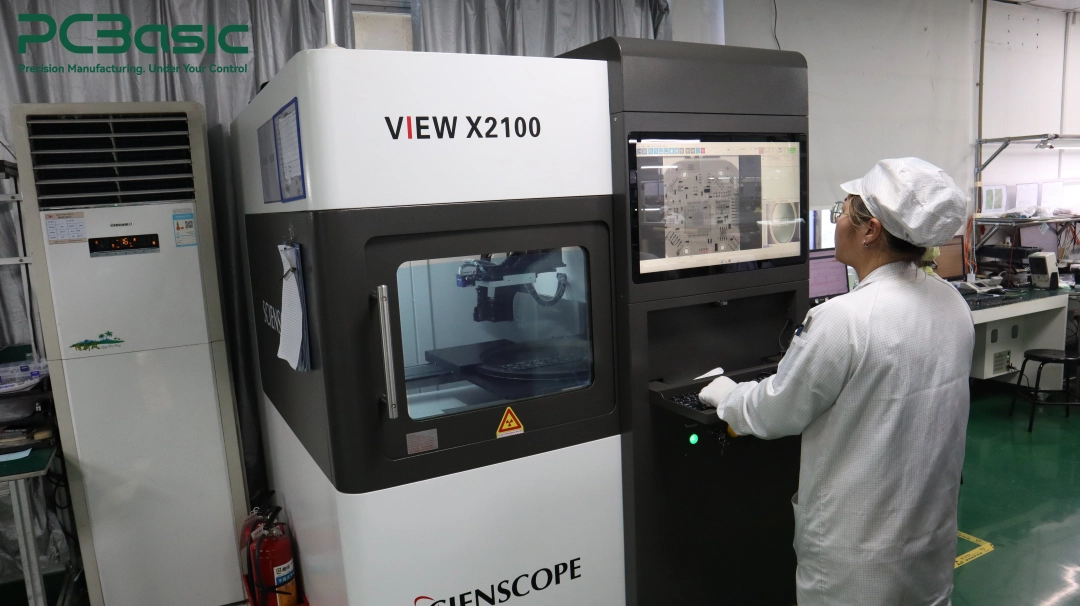
In PCBasic, we will select different inspection methods based on project requirements. Before assembly, we use SPI to check the solder paste printing situation; after reflow soldering, we use AOI to find component offsets, missing parts, and visible soldering defects. For hidden solder joints below BGA and other packaging types, X-ray can also be used for detection.
However, good solder joints do not necessarily mean the circuit will work. We can also check the electrical connections through ICT or flying probe testing and use functional testing (FCT) to verify whether the circuit board is operating normally.
For wireless module PCB assembly, the test contents need to be determined according to the product application.
For example, Bluetooth sensors may require pairing tests, GPS trackers need to check positioning and communication functions. Battery-powered devices may also need to measure the sleep current and identify abnormal power consumption.
Before the test, both parties should confirm the firmware version, power supply voltage and acceptance standards. Professional RF testing may require additional equipment and a separate test plan.
PCBasic also supports first article inspection and production traceability. It can associate the test records with production batches according to project requirements, making it convenient for subsequent quality problem investigation.

When choosing an IoT PCBA manufacturer, you should not only consider the price. Besides the cost, you also need to know whether the supplier can review your design files in advance, handle component sourcing, and complete the necessary tests for the product.
During the IoT PCB prototype assembly stage, engineers can identify some issues in advance, such as mismatch between component packaging and pads, shortage of certain materials, or unclear test requirements. If these problems are discovered only during mass production, the modifications may be more troublesome and could affect the delivery time.
If the prototype test is passed, can it be directly mass-produced? Not necessarily. Before the formal mass production, you need to confirm several issues:
• BOM and substitute components: Which BOM version to use? Who approves the substitute materials?
• First article inspection: How to confirm that the first article meets the requirements before mass production?
• Production records and communication: How to store the production records? How will both parties handle design changes or quality issues?
PCBasic supports prototypes, small batches and volume PCB assembly. Through our turnkey PCB assembly service, we can coordinate component sourcing, assembly, and testing according to the project requirements. Thus, from the prototype to mass production, you don't have to manage sourcing, assembly and testing steps separately.
Making an IoT prototype work properly is one thing, but keeping it consistent in production is another. Reliable IoT module PCB assembly services help solve these problems before manufacturing issues affect production, and ensure that component sourcing, assembly, and testing meet project requirements.
If you are developing IoT devices, you can provide Gerber files, BOM, assembly drawings, and test requirements, and contact PCBasic. We will review the specific information of the project and help you plan the next steps, whether you are making a prototype or preparing for mass production.
Q1: What is included in an IoT module PCB assembly service?
An IoT module PCB assembly service typically covers component sourcing, SMT assembly, inspection, and testing. PCB fabrication, programming, and final assembly may also be included depending on the project.
Q2: How is IoT PCB assembly different from standard PCB assembly?
IoT PCB assembly often involves compact layouts, wireless modules, sensors, and low-power circuits. These features may require additional assembly controls and functional testing.
Q3: What tests are needed for wireless IoT modules?
IoT PCB assembly testing may include electrical checks, wireless communication tests, and functional verification. GPS testing or sleep-current measurements may also be needed, depending on the device.
Q4: What files are needed for an IoT PCB assembly quote?
You'll typically need Gerber files, a BOM, and assembly drawings. Pick-and-place data, firmware files, and testing requirements may also be needed, depending on the project.
Assembly Enquiry
Instant Quote


Phone contact

+86-755-27218592
In addition, we've prepared a Help Center. We recommend checking it before reaching out, as your question and its answer may already be clearly explained there.
Wechat Support

In addition, we've prepared a Help Center. We recommend checking it before reaching out, as your question and its answer may already be clearly explained there.
WhatsApp Support

In addition, we've prepared a Help Center. We recommend checking it before reaching out, as your question and its answer may already be clearly explained there.
