Global high-mix volume high-speed PCBA manufacturer
9:00 -18:00, Mon. - Fri. (GMT+8)
9:00 -12:00, Sat. (GMT+8)
(Except Chinese public holidays)
Global high-mix volume high-speed PCBA manufacturer
9:00 -18:00, Mon. - Fri. (GMT+8)
9:00 -12:00, Sat. (GMT+8)
(Except Chinese public holidays)
HomePage > Blog > Knowledge Base > Annular Ring in PCB | A Comprehensive Guide
Annular rings are considered the central part of the PCB board, which is a circle-like structure made of copper and drilled on the board. The size and dimensions of these holes are important for designing PCB boards, helping to avoid any malfunctioning on the board. Multilayer stacks are used to design complications of boards. There is the connection of track pads of layers made by drilling small-sized holes called via. That ring helps to make good electrical connections between two different layers through copper pads. This page will discuss how these rings are made and their importance for the PCB board. Let's get started.

PCB boards come in different types based on the layers configured, including single, double, and multiple layers. On the board, there are copper layers or traces applied where different components are connected to create projects and circuits.
But for multilayer boards, different layers are connected by making small holes called vias. The vias are important for board conductivity for different layers and for accurate conductivity of the board. There is copper applied around holes, and copper around holes is known as an annular ring.
The minimum annular dimensions are one mil. But can come with different width values according to board dimensions. For proper and stable electrical connection on board, the design and manufacturing features of annular rings must be considered.
· They lie at the external layer of the PCB board and can be easily seen. It helps to make the components mount and connects the leads of components with board traces. They come with good soldering handling features and offer good electrical connections and mechanical support.
· The minimum width for annular rings on external layers of the board is 0.05 mm.
· This formula is used for outer annular ring measurements:
Outer Layer Annular Ring = (Outer Layer Pad Dia. – Plated Hole Dia.)/2
· These annular rings exist at internal layers for multilayer boards. They help to make connections of different layers through vias. For proper connection of internal layers, is accurate alignment made?
Inner Layer Annular Ring = (Inner Layer Pad Dia. – Plated Hole Dia.)/2
· The area between the external rim of the solder pad and the solder hole is called the finished annular ring. Due to drilled holes from more or less off-center annular rings, they can be broken. That is based on the external diameter of the solder pad over the diameter of the hole.

· This type of annular ring comes in a teardrop shape. For the connection of the external edges, extra copper was added in place of making a complete circle. The use of extra copper increases the ring strength.
· The main feature of these annular rings is that if the drill bit passes slightly off at the time of drilling, it can have a chance to remove copper and affect the connection.
· This type of annular ring also minimizes cracking on thin copper.
· It also controls mechanical or thermal stress and avoids any misalignments in the drill hole.
The annular ring size is significant for making accurate electrical connections of boards and design stability. The proper annular ring is important for making solder joints properly, avoiding any faults at the time of drilling, and also reducing the chances of pad lifting. The size of the annular has a direct effect on the solder joint working, conductivity, and strength of the board, especially for through-hole vias.
The proper size of rings provides uniform plating coverage and controls different problems, such as voids or thin copper layers.
Some parameters used for annular rings are
· Outer Diameter: It is the overall diameter of the pad with an annular ring and hole.
· Drilled Hole Diameter: This diameter is a hole drilled onboard.
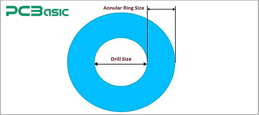
· Annular Ring Width (W): It is the radial distance between the edge of the drilled hole and the outer edge of the pad.
The annular ring size means the width of the ring made from an external point of via. The annular rings move outwards from via and come with a certain width based on the board. This formula is used for measuring annular ring size:
Annular ring = (pad dia. – finished hole dia.) / 2
The pad diameter is based on board level according to IPC-2221. That is: Level A: 24 mil, Level B: 20 mil, Level C:16 mil.
The finished hole diameter is the size of the via or its diameter.
Annular ring size is half of the difference between 2 diameters.
The minimum annular ring size for a single-layer board is 0.05mm.
The multilayer board's annular ring for inner layers is 0.1mm and for external layers is 0.05mm.
Tangency
It occurs when, by mistake, we drill a hole away from the center. If there is an off-center hole connecting the edge of the pad, it means there is a tangent issue. Another cause is that the annular ring diameter is not according to the hole.
Breakout
It is a higher type of tangent and occurs when the hole is drilled that goes out from the annular ring. So the annular ring is cut off and results in a breakout. To solve this issue, readjust the machine.
Rupture
Due to extensive use or at the time of drilling, annular rings get damaged, which is known as rupture. To avoid this issue, use quality raw materials and thick copper pads.

Pad Lifting
If the pad along the annular ring is disconnected from the PCB substrate, it causes a pad lifting issue. That is the result of thermal cycling and mechanical stress. To solve this issue, use materials and processes that provide adhesion and avoid high heat production when manufacturing the board.
1. Design Considerations
· The width of the annular ring must be accurate according to the design. Normally, the thickness is 0.15 mm for standard uses, but it can be set according to the board layer and thickness.
· The pad must have a higher diameter compared to the hole diameter. Normally 1.5 times the drill size.
2. Drilling Accuracy
· There is a need for proper drill size based on annular ring parameters. To avoid the burr creation, use high-quality drill bits. That is good for maintaining the proper annular ring width.
The annular rings are the main factor that helps design the PCB board, which provides accurate electrical and mechanical connections for different connected components. The accurate design of these rings is best for the proper working of the board, and their design has tolerance for board manufacturing to follow the different industry rules for saving the board quality. The accurate configuration of these rings helps to provide a high-strength board made with through-hole technology. For high-speed circuit design, they are important for impedance matching and provide high-quality signals.
 About PCBasic
Time is money in your projects – and PCBasic gets it. PCBasic is a PCB assembly company that delivers fast, flawless results every time. Our comprehensive PCB assembly services include expert engineering support at every step, ensuring top quality in every board. As a leading PCB assembly manufacturer, we provide a one-stop solution that streamlines your supply chain. Partner with our advanced PCB prototype factory for quick turnarounds and superior results you can trust.

Assembly Enquiry
Instant Quote
Phone contact

+86-755-27218592
In addition, we've prepared a Help Center. We recommend checking it before reaching out, as your question and its answer may already be clearly explained there.
Wechat Support

In addition, we've prepared a Help Center. We recommend checking it before reaching out, as your question and its answer may already be clearly explained there.
WhatsApp Support

In addition, we've prepared a Help Center. We recommend checking it before reaching out, as your question and its answer may already be clearly explained there.