Global high-mix volume high-speed PCBA manufacturer
9:00 -18:00, Mon. - Fri. (GMT+8)
9:00 -12:00, Sat. (GMT+8)
(Except Chinese public holidays)
Global high-mix volume high-speed PCBA manufacturer
9:00 -18:00, Mon. - Fri. (GMT+8)
9:00 -12:00, Sat. (GMT+8)
(Except Chinese public holidays)
The layout of your PCB is unclear. If the outline or board layout is not clearly defined, it may lead to incorrect PCB fabrication.
There are usually two common situations causing this issue:
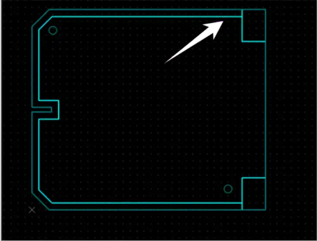
1. Multiple Outlines on the Same or Different Layers
When there are several PCB outlines on one or more layers (such as GKO, GM1, or other mechanical layers), our engineers cannot identify which one represents the actual board edge.
→ Please delete the redundant outlines or add a clear note indicating which layer should be considered as the final outline (e.g., “Outline is GM1” or “Use GKO layer as final outline”).

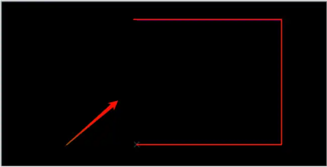
2. Incomplete Outline
As shown in the screenshot below, the board outline is partially missing — for example, one side is not closed. In such cases, it’s hard to determine whether the PCB should be a regular rectangle or have special notches or irregular edges.
→ Please complete the outline and re-upload the corrected Gerber file for review.
If your design only includes four corner markers and you intend for the edges to be connected with straight lines (without notches), please add a remark when creating the order so PCBasic can confirm and process it correctly.

Phone contact

+86-755-27218592
In addition, we've prepared a Help Center. We recommend checking it before reaching out, as your question and its answer may already be clearly explained there.
Wechat Support

In addition, we've prepared a Help Center. We recommend checking it before reaching out, as your question and its answer may already be clearly explained there.
WhatsApp Support

In addition, we've prepared a Help Center. We recommend checking it before reaching out, as your question and its answer may already be clearly explained there.