Global high-mix volume high-speed PCBA manufacturer
9:00 -18:00, Mon. - Fri. (GMT+8)
9:00 -12:00, Sat. (GMT+8)
(Except Chinese public holidays)
Global high-mix volume high-speed PCBA manufacturer
9:00 -18:00, Mon. - Fri. (GMT+8)
9:00 -12:00, Sat. (GMT+8)
(Except Chinese public holidays)
HomePage > Blog > Knowledge Base > PCB Surface Finish Types: A Comprehensive Guide
Surface finish is a very important step in the production of circuit boards. This is because the reliability of PCBs largely depends on the protective coating on the pad surface. If there is no appropriate surface finish, the copper surface will oxidize rapidly, resulting in a decline in solderability and seriously affecting the performance and lifespan of the product. Therefore, it is very necessary to understand the relevant knowledge about surface finish.
There are various surface finish methods, each with its own characteristics. Some are low-cost and convenient for soldering, but have average durability; others, although more expensive, can ensure longer-term stability. Therefore, when choosing the type of PCB surface finish, a balance usually needs to be struck among multiple aspects, such as price, durability, and soldering quality.
Next, in this article, we will delve into several of the most common PCB surface finish methods and analyze their advantages and disadvantages. A thorough understanding of these PCB surface finish methods will be beneficial for making more reasonable design and material selection decisions, thereby enhancing overall manufacturing efficiency and product competitiveness. First of all, let's start by understanding the definition of PCB surface finish.
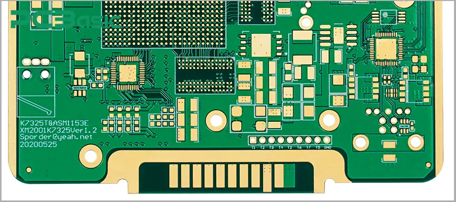
PCB surface finish refers to the application of a protective coating on the exposed copper pads of the PCB. Its function is to prevent copper oxidation and maintain good solderability. Thus, during the assembly process, it can provide a stable soldering interface for components. Nowadays, according to the different requirements of products, various types of PCB surface finish processes have been developed. For example, the lead-free HASL process widely used in consumer products, and the high-performance ENIG, ENEPIG or hard gold processes used in high-end applications.
Surface finish is not an optional process but an indispensable key link in PCB production. As mentioned at the beginning, the bare copper on the circuit board is prone to reacting with the air and oxidizing rapidly. Once oxidized, it will seriously reduce solderability, causing poor solder wetting and false soldering of the solder joints. Therefore, it is necessary to adopt appropriate PCB surface finish to ensure that the copper surface remains good solderability throughout the storage, assembly and entire life cycle of the product.
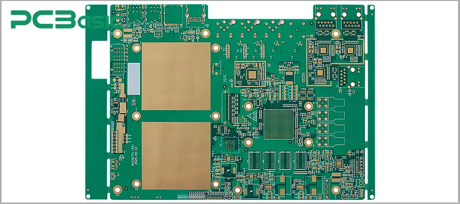
In summary, the necessity of PCB surface finish mainly lies in the following aspects:
1. Copper surface finish can effectively prevent air and moisture from reaching the copper surface, thus avoiding the loss of luster and electrical performance of the copper surface.
2. Modern assembly processes such as SMT and BGA have extremely high requirements for the consistency of the pad surface. Without surface finish, the solder paste cannot fully wet the pad, which can easily cause short circuits, open circuits or false soldering.
3. A PCB surface with high flatness is particularly important for the current mainstream high-density packaging such as BGA/QFN.
4. Surface finish can extend the shelf life of the board and ensure that the board still has stable solderability after a long period of time. Thus, there is no problem if the PCB is stored for a long time before assembly.
5. Surface finishes such as ENEPIG or hard gold can provide excellent wear resistance and stable electrical performance, ensuring long-term reliability even after many years.
From this, it is evident that surface finish is of great significance in PCB manufacturing.
Different PCB surface finish processes vary depending on the product category, cost requirements, reliability standards, and environmental regulations. Some of these processes are mainstream in the industry and are widely used in consumer electronics, industrial control, and high-reliability fields. Next, we will elaborate on several common PCB surface finish types.
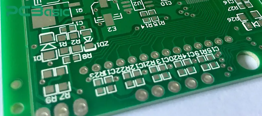
Hot Air Solder Leveling (HASL) is one of the most classic and widely used PCB surface finish processes. This process involves immersing the circuit board in molten solder, followed by using a hot air knife to remove the excess solder, thereby forming a protective layer on the surface of the solder pads. Depending on the type of solder used, HASL can be classified as HASL with lead and lead free HASL.
Over the past few decades, HASL with lead was the most common PCB surface finish process worldwide. Due to its simple process, low cost, and good solderability, it was widely used. However, later, because of the presence of lead in the process, it did not meet the RoHS environmental standards, and the surface flatness of the solder pads was poor, making it unsuitable for high-density assembly and its usage gradually decreased.
To address the environmental protection issue, lead-free HASL emerged accordingly. This process uses a lead-free tin alloy instead of lead-containing solder, and is widely used in consumer electronics, industrial control, and automotive PCBs. It not only maintains good solderability but also complies with the RoHS regulations. However, this process requires a higher processing temperature, and it will also cause thermal stress on multi-layer boards. Moreover, its flatness is not as advanced as processes such as ENIG.
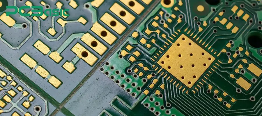
ENIG is one of the most popular PCB surface finish methods at present. Its process mainly consists of two steps: first, a layer of nickel is deposited on the copper surface as a barrier layer; then, a thin layer of gold is deposited on the nickel layer. The purpose of the nickel layer is to prevent copper from diffusing into the solder joints, and the gold layer provides protection and maintains good solderability.
The greatest advantage of this process is its excellent surface flatness, which is very suitable for fine-pitch packaging such as BGA and QFN, and is widely used in high-reliability products. In addition, it also has excellent oxidation resistance and a long shelf life, which is very practical for PCB production of smartphones, laptops, servers, and high-reliability industrial equipment.
The drawback is that its cost is relatively high. Moreover, if the process control is improper, the black pad* defect may occur. Despite these risks, ENIG remains the preferred choice for the surface of high-end PCBs.
*Black pad refers to a dark black corrosion layer that appears on the nickel surface during the ENIG process. This layer is point-like or strip-like in distribution and results from poor control of the chemical nickel plating process (such as excessive phosphorus content or excessive corrosion effect). This will,
Hinder the normal bonding of solder and nickel;
Result in a decrease in the strength of the solder joint, making it prone to cracking or poor soldering;
Causes the soldering to fail and the board to be scrapped in severe cases.
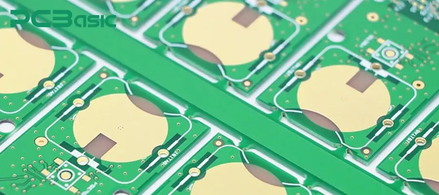
ENEPIG is currently the most advanced method of PCB surface finish. It builds upon ENIG by adding a layer of palladium between the nickel and gold. The added palladium layer effectively prevents corrosion, eliminates the risk of black spots, and significantly improves the bonding performance, enabling it to be compatible with both gold and aluminum wires for soldering.
ENEPIG boasts extremely high reliability, outstanding solder joint strength, and excellent wire bonding performance. It is increasingly being used in fields such as aerospace, medical devices, and military electronics, where reliability is of utmost importance. However, this process is costly, complex, and requires strict quality control. If your product emphasizes performance and lifespan, then ENEPIG is the best choice.
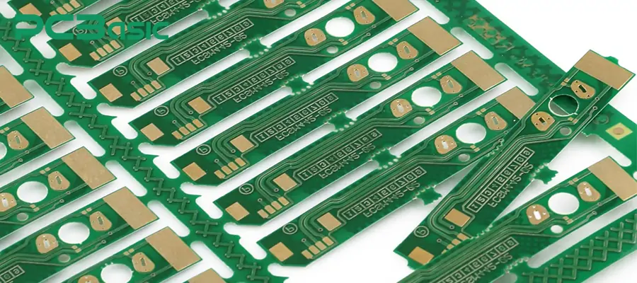
OSP is another common surface finish process. This process involves covering the surface of copper pads with an organic protective film to prevent copper oxidation until the soldering is completed. Unlike metal coatings, the protective film in OSP is transparent and extremely thin.
This process has the advantages of low cost, smooth surface, and environmental friendliness. It can provide an extremely smooth copper surface finish, which is very suitable for the assembly of fine-pitch components, and fully complies with RoHS standards. It is commonly used in PC motherboards, consumer electronics, and mass industrial products.
The disadvantage is that the shelf life is short, it is sensitive to the operating environment and surface cleanliness, and its performance will decline after multiple reflow soldering. This indicates that OSP is suitable for one-time assembly and consumer products with a short life cycle.
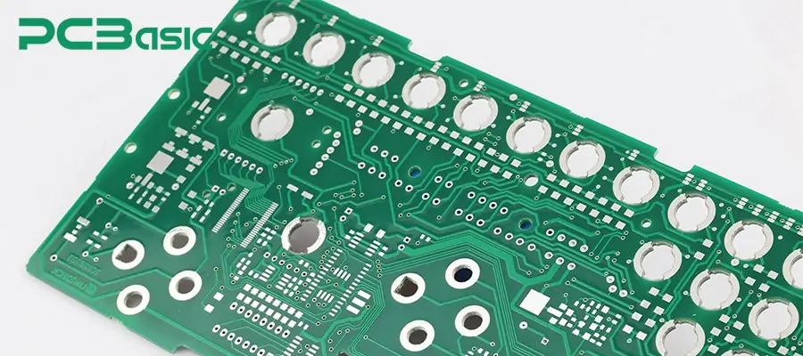
Immersion silver plating involves depositing a thin layer of silver directly onto the copper surface. This process has excellent solderability and flatness, as well as excellent electrical conductivity, making it highly suitable for high-frequency circuits and communication products. Its cost is lower than ENIG, but it is prone to oxidation and discoloration, and has a limited shelf life.
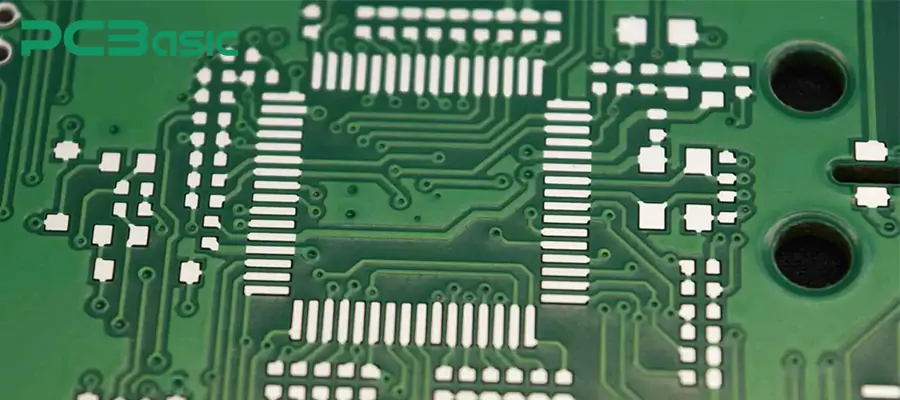
Immersion tin is a process where a layer of tin is deposited on the copper surface through chemical means, creating a smooth and solderable surface. This PCB surface finish is lead-free, complies with RoHS requirements, and is suitable for the soldering of fine-pitch components. However, it is prone to the formation of tin whiskers, which can cause short circuits, and has limited durability.
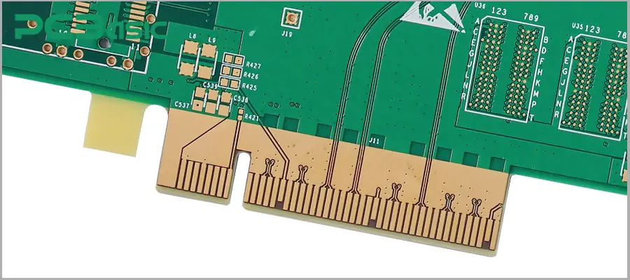
Hard gold is also known as electrolytic nickel gold, abbreviated as ENEG. This process involves first plating nickel on the copper surface and then electrolytically plating gold to form a thick and wear-resistant coating. It is one of the most durable PCB surface finishes and is commonly used in high-wear areas such as gold fingers and connectors. But its cost is extremely high, and the hardness is too great, making it unsuitable for ordinary solder joints. It is often used in combination with other PCB surface finish types.
Now, we will compare several common PCB surface finish methods.
HASL vs. ENIG
Feature / Factor
HASL
ENIG
Cost
Very low (HASL with lead is the cheapest; lead free HASL slightly higher)
Higher cost
Flatness
Uneven surface; not ideal for BGAs/QFNs
Very flat, excellent for BGAs & fine-pitch
Solderability
Good; easy to rework
Excellent; stable during multiple reflows
Environmental Compliance
HASL with lead = Not RoHS compliant;
HASL lead free = RoHS compliant
RoHS compliant
Durability / Shelf Life
Moderate, limited storage life
Long shelf life, oxidation-resistant
Typical Applications
Consumer, industrial, cost-sensitive boards
High-reliability electronics: smartphones, servers, medical devices
ENIG vs. ENEPIG
|
Feature / Factor |
ENIG |
ENEPIG |
|
Cost |
High |
Very high |
|
Flatness |
Excellent |
Excellent |
|
Oxidation Resistance |
Very good |
Excellent |
|
Black Pad Risk |
Possible if process poorly controlled |
Eliminated |
|
Wire Bonding |
Limited |
Excellent (gold/aluminum wires) |
|
Reliability |
High |
Extremely high |
|
Applications |
Consumer electronics, automotive, industrial |
Aerospace, defense, medical, and high-end products |
Hard Gold vs. Immersion Gold
|
Feature / Factor |
Hard Gold |
Immersion Gold |
|
Cost |
Very high |
Moderate (within ENIG process) |
|
Thickness |
Thick, durable gold layer |
Thin immersion gold layer |
|
Durability |
Excellent wear resistance (connectors, fingers) |
Not for wear; protects nickel & solderability |
|
Solderability |
Poor (too hard for reliable solder joints) |
Excellent for SMT/BGA assembly |
|
Applications |
Edge connectors, keypads, high-contact areas |
General assembly, fine-pitch components |
There is no absolute best or worst among different PCB surface finish types. When making a choice, what we need to do is to find a balance among cost, flatness, durability and application requirements. So, how to choose the right surface finish for your PCBs? When making a choice, we can focus on the following aspects:
1. Application scenario requirements
For example, for consumer electronics that are sensitive to costs, lead-free HASL or OSP are usually the most suitable choices, as they offer favorable prices and good reliability. For high-density or high-speed circuits with strict requirements for flatness and signal integrity, ENIG or immersion silver is a better option.
2. Cost budget
For example, HASL with lead has the lowest cost, but it no longer complies with RoHS.
Lead-free HASL strikes a balance between price and compliance.
ENEPIG and hard gold have the highest cost, but are suitable for high-end products.
3. Durability requirements
For connectors that are frequently plugged and unplugged, gold fingers → choose hard gold (Hard Gold).
For ordinary welding areas → choose ENIG or lead-free HASL.
4. Environmental protection and regulatory compliance
If the process is required to comply with environmental protection and regulations, then it is necessary to ensure that the selected PCB surface finish meets standards such as RoHS, REACH, etc. HASL with lead is definitely not an option.
Each process has its own advantages and limitations. There is no "optimal" PCB surface finish type that is suitable for all situations. We need to find a balance among cost, flatness, durability and compliance based on the application requirements, in order to select the most suitable surface finish method.
 About PCBasic
Time is money in your projects – and PCBasic gets it. PCBasic is a PCB assembly company that delivers fast, flawless results every time. Our comprehensive PCB assembly services include expert engineering support at every step, ensuring top quality in every board. As a leading PCB assembly manufacturer, we provide a one-stop solution that streamlines your supply chain. Partner with our advanced PCB prototype factory for quick turnarounds and superior results you can trust.
Assembly Enquiry
Instant Quote
Phone contact

+86-755-27218592
In addition, we've prepared a Help Center. We recommend checking it before reaching out, as your question and its answer may already be clearly explained there.
Wechat Support

In addition, we've prepared a Help Center. We recommend checking it before reaching out, as your question and its answer may already be clearly explained there.
WhatsApp Support

In addition, we've prepared a Help Center. We recommend checking it before reaching out, as your question and its answer may already be clearly explained there.